Features: ` Power Dissipation . . . 40 mW Max
` Advanced LinEPIC™Single-Poly Process Provides Close Capacitor Matching for Better Accuracy
` Fast Parallel Processing for DSP and P Interface
` Either External or Internal Clock Can Be Used
` Conversion Time . . . 6 s
` Total Unadjusted Error . . . ±1 LSB Max
` CMOS TechnologyPinout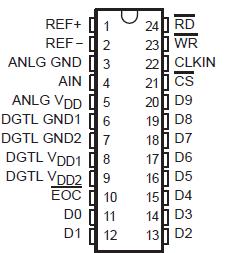 Specifications
Supply voltage, VDD1, VDD2, and VDD3 (see Note 1) . . . . . . . . . . . . . . . . . . . . . . . . . . . . .. . . . . . . 6.5 V
Input voltage range, VI (any input) . . . . . . . . . . . . . . . . . . . . . . . . . . . . . . . . .. . . −0.3 V to VDD + 0.3 V
Output voltage range, VO . . . . . . . . . . . . . . . . . . . . . . . . . . . . . . . . . . . . . . . . . . . −0.3 V to VDD + 0.3 V
Peak input current (any digital input) . . . . . . . . . . . . . . . . . . . . . . . . . . . . . . . . . . . . . . . . . . . . . ±10 mA
Peak total input current (all inputs) . . . . . . . . . . . . . . . . . . . . . . . . . . . . . . . . . . . . . . . . . . . . . . ±30 mA
Operating free-air temperature range, TA: TLC1550I, TLC1551I . . . ................................. .−40 to 85
TLC1550M . . . . . . . . . ... ............................... −55 to 125
Storage temperature range, Tstg . . . . . . . . . . . . . . . . . . . . . . . . . . . . . . . . . . . . . . . . . .. . −65 to 150
Case temperature for 10 seconds: FK or FN package . . . . . . . . . . . . . . . . . . . . . . . . . . . . . . . . . . . 260
Lead temperature 1,6 mm (1/16 inch) from the case for 10 seconds: J or NW package . . . . .. . . . . 260
† Stresses beyond those listed under "absolute maximum ratings" may cause permanent damage to the device. These are stress ratings only, and functional operation of the device at these or any other conditions beyond those indicated under "recommended operating conditions" is not implied. Exposure to absolute-maximum-rated conditions for extended periods may affect device reliability.
NOTE 1: VDD1 is the voltage measured at DGTL VDD1 with respect to DGND1. VDD2 is the voltage measured at DGTL VDD2 with respect to the DGND2. VDD3 is the voltage measured at ANLG VDD with respect to AGND. For these specifications, all ground terminals are tied together (and represent 0 V). When VDD1, VDD2, and VDD3 are equal, they are referred to simply as VDD.
DescriptionThe TLC1550x and TLC1551 are data acquisition analog-to-digital converters (ADCs) using a 10-bit, switched-capacitor, successive-approximation network. A high-speed, 3-state parallel port directly interfaces to a digital signal processor (DSP) or microprocessor (P) system data bus. D0 through D9 are the digital output terminals with D0 being the least significant bit (LSB). Separate power terminals for the analog and digital portions minimize noise pickup in the supply leads. Additionally, the digital power is divided into two parts to separate the lower current logic from the higher current bus drivers. An external clock can be applied to CLKIN to override the internal system clock if desired.
The TLC1550x and TLC1551 are characterized for operation from −40°C to 85°C. The TLC1550M is characterized over the full military range of −55°C to 125°C.

 TCL1551I Data Sheet


