TDA4670

Features: · Luminance signal delay from 20 to 1100 ns (minimum step 45 ns)· Luminance signal peaking with selectable symmetrical overshoots· 2.6 or 5 MHz peaking centre frequency and selectable degree of peaking (-3, 0, +3 and +6 dB)· Selectable noise reduction by coring· Handles negative and posi...

product image

TDA4670 Picture
SeekIC No. : 004516369 Detail

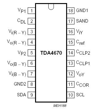
TDA4670: Features: · Luminance signal delay from 20 to 1100 ns (minimum step 45 ns)· Luminance signal peaking with selectable symmetrical overshoots· 2.6 or 5 MHz peaking centre frequency and selectable degr...

floor Price/Ceiling Price

Part Number:
TDA4670
Supply Ability:
5000

Price Break

  • Qty
  • 1~5000
  • Unit Price
  • Negotiable
  • Processing time
  • 15 Days
Total Cost: $ 0.00

SeekIC Buyer Protection PLUS - newly updated for 2013!

  • Escrow Protection.
  • Guaranteed refunds.
  • Secure payments.
  • Learn more >>

Month Sales

268 Transactions

Rating

evaluate  (4.8 stars)

Upload time: 2024/5/14

Payment Methods

All payment methods are secure and covered by SeekIC Buyer Protection PLUS.

Notice: When you place an order, your payment is made to SeekIC and not to your seller. SeekIC only pays the seller after confirming you have received your order. We will also never share your payment details with your seller.
Product Details

Description


Features:

· Luminance signal delay from 20 to 1100 ns (minimum step 45 ns)
· Luminance signal peaking with selectable symmetrical overshoots
· 2.6 or 5 MHz peaking centre frequency and selectable degree of peaking (-3, 0, +3 and +6 dB)
· Selectable noise reduction by coring
· Handles negative and positive colour-difference signals
· Selectable Colour Transient Improvement (CTI) to decrease the colour-difference signal transient times to those of the high frequency luminance signals
· Selectable 5 or 12 V sandcastle input voltage
· All controls selected via the I2C-bus
· Timing pulse generation for clamping and delay time control synchronized by sandcastle pulse
· Automatic luminance signal delay correction using a control loop
· Luminance and colour-difference input signal clamping with coupling capacitor
· 4.5 to 8.8 V supply voltage range
· Minimum of external components required.


Pinout

  Connection Diagram


Specifications

SYMBOL PARAMETER CONDITIONS MIN. MAX. UNIT
VP1 supply voltage (pin 1)   0 8.8 V
VP2 supply voltage (pin 5)   0 8.8 V
Ptot total power dissipation   0 0.97 mA
Tstg storage temperature   -25 +150 A
Tamb operating ambient temperature   0 70
VESD electrostatic handling
for pins 9 and 10
for other pins
note 1 -
-
-
+300
-500
±500
V
V
V
Note
1. Equivalent to discharging a 200 pF capacitor through a 0 series resistor.


Description

The TDA4670 delays the luminance signal and improves colour-difference signal transients. Additionally, the luminance signal can be improved by peaking and noise reduction (coring).


Customers Who Bought This Item Also Bought

Margin,quality,low-cost products with low minimum orders. Secure your online payments with SeekIC Buyer Protection.
Discrete Semiconductor Products
Transformers
Memory Cards, Modules
Cables, Wires - Management
Static Control, ESD, Clean Room Products
Audio Products
View more