TL080

Features: • Low-Power Consumption• Wide Common-Mode and Differential Voltage Ranges• Low Input Bias and Offset Currents• Output Short-Circuit Protection• Low Total Harmonic Distortion . . . 0.003% Typ• High Input Impedance . . . JFET-Input Stage• Internal ...

product image

TL080 Picture
SeekIC No. : 004520002 Detail

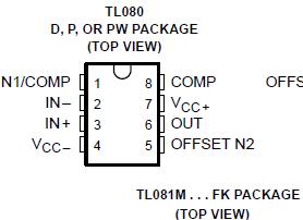
TL080: Features: • Low-Power Consumption• Wide Common-Mode and Differential Voltage Ranges• Low Input Bias and Offset Currents• Output Short-Circuit Protection• Low Total Harm...

floor Price/Ceiling Price

Part Number:
TL080
Supply Ability:
5000

Price Break

  • Qty
  • 1~5000
  • Unit Price
  • Negotiable
  • Processing time
  • 15 Days
Total Cost: $ 0.00

SeekIC Buyer Protection PLUS - newly updated for 2013!

  • Escrow Protection.
  • Guaranteed refunds.
  • Secure payments.
  • Learn more >>

Month Sales

268 Transactions

Rating

evaluate  (4.8 stars)

Upload time: 2024/4/26

Payment Methods

All payment methods are secure and covered by SeekIC Buyer Protection PLUS.

Notice: When you place an order, your payment is made to SeekIC and not to your seller. SeekIC only pays the seller after confirming you have received your order. We will also never share your payment details with your seller.
Product Details

Description


Features:

• Low-Power Consumption
• Wide Common-Mode and Differential Voltage Ranges
• Low Input Bias and Offset Currents
• Output Short-Circuit Protection
• Low Total Harmonic Distortion . . . 0.003% Typ
• High Input Impedance . . . JFET-Input Stage
• Internal Frequency Compensation (Except TL080, TL080A)
• Latch-Up-Free Operation
• High Slew Rate . . . 13 V/ms Typ
• Common-Mode Input Voltage Range Includes VCC+


Pinout

  Connection Diagram


Specifications

 
TL08_C
TL08_AC
TL08_BC
TL08_I
TL08_M
UNIT
Supply voltage, VCC+ (see Note 1)
18
18
18
V
Supply voltage VCC (see Note 1)
18
18
18
V
Differential input voltage (see Note 2)
± 30
± 30
± 30
V
Input voltage (see Notes 1 and 3)
±15
±15
±15
V
Duration of output short circuit (see Note 4)
unlimited
unlimited
unlimited
Continuous total dissipation
See Dissipation Rating Table
Operating free-air temperature range
0 to 70
40 to 85
55 to 125
°C
Storage temperature range
65 to 150
65 to 150
65 to 150
°C
Case temperature for 60 seconds FK package
260
°C
Lead temperature 1,6 mm (1/16 inch)
from case for 60 seconds
J or JG package
300
°C
Lead temperature 1,6 mm (1/16 inch)
from case for 10 seconds
D, N, P, or PW package
260
260
°C
NOTES: 1. All voltage values, except differential voltages, are with respect to the midpoint between VCC+ and VCC.
2. Differential voltages are at the noninverting input terminal with respect to the inverting input terminal.
3. The magnitude of the input voltage must never exceed the magnitude of the supply voltage or 15 V, whichever is less.
4. The output may be shorted to ground or to either supply. Temperature and/or supply voltages must be limited to ensure that the dissipation rating is not exceeded.


Description

The TL08_ JFET-input operational amplifier family is designed to offer a wider selection than any previously developed operational amplifier family. Each of these JFET-input operational amplifiers incorporates well-matched, high-voltage JFET and bipolar transistors in a monolithic integrated circuit. The devices feature high slew rates, low input bias and offset currents, and low offset voltage temperature coefficient. Offset adjustment and external compensation options are available within the TL08_ family.

Device types with a C suffix are characterized for operation from 0°C to 70°C, those with an I suffix are characterized for operation from 40°C to 85°C, and those with an M suffix are characterized for operation over the full military temperature range of 55°C to 125°C.


Customers Who Bought This Item Also Bought

Margin,quality,low-cost products with low minimum orders. Secure your online payments with SeekIC Buyer Protection.
Circuit Protection
Industrial Controls, Meters
Inductors, Coils, Chokes
Optoelectronics
Static Control, ESD, Clean Room Products
View more