TLC372

Features: Single or Dual-Supply OperationWide Range of Supply Voltages 2 V to 18 VLow Supply Current Drain 150 µA Typ at 5 VFast Response Time . . . 200 ns Typ for TTL-Level Input StepBuilt-in ESD ProtectionHigh Input Impedance . . . 1012 Ω TypExtremely Low Input Bias Current 5 pA TypU...

product image

TLC372 Picture
SeekIC No. : 004520630 Detail

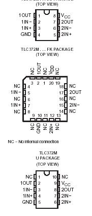
TLC372: Features: Single or Dual-Supply OperationWide Range of Supply Voltages 2 V to 18 VLow Supply Current Drain 150 µA Typ at 5 VFast Response Time . . . 200 ns Typ for TTL-Level Input StepBuilt-in...

floor Price/Ceiling Price

Part Number:
TLC372
Supply Ability:
5000

Price Break

  • Qty
  • 1~5000
  • Unit Price
  • Negotiable
  • Processing time
  • 15 Days
Total Cost: $ 0.00

SeekIC Buyer Protection PLUS - newly updated for 2013!

  • Escrow Protection.
  • Guaranteed refunds.
  • Secure payments.
  • Learn more >>

Month Sales

268 Transactions

Rating

evaluate  (4.8 stars)

Upload time: 2024/4/25

Payment Methods

All payment methods are secure and covered by SeekIC Buyer Protection PLUS.

Notice: When you place an order, your payment is made to SeekIC and not to your seller. SeekIC only pays the seller after confirming you have received your order. We will also never share your payment details with your seller.
Product Details

Description


Features:

 Single or Dual-Supply Operation
 Wide Range of Supply Voltages 2 V to 18 V
 Low Supply Current Drain 150 µA Typ at 5 V
 Fast Response Time . . . 200 ns Typ for TTL-Level Input Step
 Built-in ESD Protection
 High Input Impedance . . . 1012 Ω Typ
 Extremely Low Input Bias Current 5 pA Typ
 Ultrastable Low Input Offset Voltage
 Input Offset Voltage Change at Worst-Case Input Conditions Typically 0.23 µV/Month,Including the First 30 Days
 Common-Mode Input Voltage Range Includes Ground
 Output Compatible With TTL, MOS, and CMOS
 Pin-Compatible With LM393


Pinout

  Connection Diagram


Specifications

Supply voltage, VDD (see Note 1)  . . . . . . . . . . . . . . . . . . . . . . . . . . . . .18 V
Differential input voltage, VID (see Note 2  . . . . . . . . . . . . . . . . . . . .  . .±18 V
Input voltage range, VI . . . . . . . . . . . . . . . . . . . . . . . . . . . . . . . . . . . . .0.3 V to 18 V
Output voltage, VO  . . . . . . . . . . . . . . . . . . . . . . . . . . . . . . . . . . . . . . . . .18 V
Input current, II . . . . . . . . . . . . . . . . . . . . . . . . . . . . . . . . . . . . . . . . . .. . .±5 mA
Output current, IO  . . . . . . . . . . . . . . . . . . . . . . . . . . . . . . . . . . . . . . . .. . . .20 mA
Duration of output short circuit to ground (see Note 3) . . . . . . . . . . . . .unlimited
Package thermal impedance, JA (see Notes 4 and 5): D package  . . . .. .97.1°C/W
                                                                                      P package . . . . . . . . 84.6°C/W
                                                                                      PW package  . . . . . ..149°C/W
Package thermal impedance, JC (see Notes 4 and 5): FK package . . . . . . .5.6°C/W
                                                                                       JG package  . . . . . . .14.5°C/W
                                                                                      U package . . . . . . . .14.7°C/W
Operating free-air temperature range, TA:TLC372C . . . . . . . . . . . . . . . . .0°C to 70°C 
                                                                  TLC372I  . . . . . . . . . . . . . . −40°C to 85°C
                                                                  TLC372M . . . . . . . . . . . . . .−55°C to 125°C
                                                                  TLC372Q  . . . . . . . . . . . . .−40°C to 125°C
Storage temperature range  . . . . . . . . . . . . . . . . . . . . . . . . . . . . . . .−65°C to 150°C
Case temperature for 60 seconds: FK package . . . . . . . . . . . . . . . . . . . . . 260°C
Lead temperature 1,6 mm (1/16 inch) from
 case for 10 seconds: D, P, or PW package  .    . . . . . . . . . .                       260°C
Lead temperature 1,6 mm (1/16 inch) from
case for 60 seconds: JG or U package  . . . . . . . . . . . . . .  . . . . . .               300°C


Description

  This TLC372 is fabricated using LinCMOStechnology and consists of two independent voltage comparators, each designed to operate from a single power supply. Operation from dual supplies is also possible if the difference between the two supplies is 2 V to 18 V. Each device TLC372 features extremely high input impedance (typically greater than 1012 Ω), allowing direct interfacing with high-impedance sources. The outputs are n-channel open-drain configurations and can be connected to achieve positive-logic wired-AND relationships.

  The TLC372 has internal electrostatic discharge (ESD) protection circuits and has been classified with a 1000-V ESD rating using human body model testing. However, care should be exercised in handling this device as exposure to ESD may result in a degradation of the device parametric performance.


Customers Who Bought This Item Also Bought

Margin,quality,low-cost products with low minimum orders. Secure your online payments with SeekIC Buyer Protection.
Programmers, Development Systems
Cables, Wires
Computers, Office - Components, Accessories
Connectors, Interconnects
Optical Inspection Equipment
Hardware, Fasteners, Accessories
View more