TLV277xA

Features: * High Slew Rate ...10.5 V/s Typ* High-Gain Bandwidth ...5.1 MHz Typ* Supply Voltage Range 2.5 V to 5.5 V* Rail-to-Rail Output* 360V Input Offset Voltage* Low Distortion Driving 600- 0.005% THD+N* 1 mA Supply Current (Per Channel)* 17 nV/Hz Input Noise Voltage* 2 pA Input Bias Current* C...

product image

TLV277xA Picture
SeekIC No. : 004522402 Detail

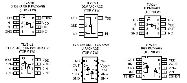
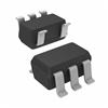
TLV277xA: Features: * High Slew Rate ...10.5 V/s Typ* High-Gain Bandwidth ...5.1 MHz Typ* Supply Voltage Range 2.5 V to 5.5 V* Rail-to-Rail Output* 360V Input Offset Voltage* Low Distortion Driving 600- 0.005...

floor Price/Ceiling Price

Part Number:
TLV277xA
Supply Ability:
5000

Price Break

  • Qty
  • 1~5000
  • Unit Price
  • Negotiable
  • Processing time
  • 15 Days
Total Cost: $ 0.00

SeekIC Buyer Protection PLUS - newly updated for 2013!

  • Escrow Protection.
  • Guaranteed refunds.
  • Secure payments.
  • Learn more >>

Month Sales

268 Transactions

Rating

evaluate  (4.8 stars)

Upload time: 2024/4/25

Payment Methods

All payment methods are secure and covered by SeekIC Buyer Protection PLUS.

Notice: When you place an order, your payment is made to SeekIC and not to your seller. SeekIC only pays the seller after confirming you have received your order. We will also never share your payment details with your seller.
Product Details

Description


Features:

* High Slew Rate ...10.5 V/s Typ
* High-Gain Bandwidth ...5.1 MHz Typ
* Supply Voltage Range 2.5 V to 5.5 V
* Rail-to-Rail Output
* 360V Input Offset Voltage
* Low Distortion Driving 600-
   0.005% THD+N
* 1 mA Supply Current (Per Channel)
* 17 nV/Hz Input Noise Voltage
* 2 pA Input Bias Current
* Characterized From T = -55 to 125
* Available in MSOP and SOT-23 Packages
* Micropower Shutdown Mode ...IDD < 1 A
* Available in Q-Temp Automotive
   High Reliability Automotive Applications
   Configuration Control / Print Support
   Qualification to Automotive Standards


Pinout

  Connection Diagram


Specifications

Supply voltage, VDD (see Note 1). . . . . . . . . . . . . . . . . . . . . . . . . . . . . . . . . . . . . . . . . . . . . . . . . . . . . . . . . 7 V
Differential input voltage, VID (see Note 2) . . . . . . . . . . . . . . . . . . . . . . . . . . . . . . . . . . . . . . . . . . . . . . . .±VDD
Input voltage range, VI (any input, see Note 1) . . . . . . . . . . . . . . . . . . . . . . . . . . . . . . . . ... . . . .0.3 V to VDD
Input current, II (any input) . . . . . . . . . . . . . . . . . . . . . . . . . . . . . . . . . . . . . . . . . . . . . . . . . . . . . . . . . . .±4 mA
Output current, IO . . . . . . . . . . . . . . . . . . . . . . . . . . . . . . . . . . . . . . . . . . . . . . . . . . . . . . . . . .  . . . . . . .±50 mA
Total current into VDD+ . . . . . . . . . . . . . . . . . . . . . . . . . . . . . . . . . . . . . . . . . . . . . . . . . . . . . . . . . . . . . .±50 mA
Total current out of GND . . . . . . . . . . . . . . . . . . . . . . . . . . . . . . . . . . . . . . . . . . . . . . . . . . . . . . . . . . . . .±50 mA
Duration of short-circuit current (at or below) 25 (see Note 3). . . . . . . . . . . . . . . . . . . . . . . . . . .. . . unlimited
Continuous total power dissipation . . . . . . . . . . . . . . . . . . . . . . . . . . . . . . .  . . . . .See Dissipation Rating Table
Operating free-air temperature range, TA: C suffix  . . . . . . . . . . . . . . . . . . . . . . . . . . . . . . .. . . . . . . .0 to 70
                                                                   I suffix . . . . . . . . . . . . . . . . . . . . . . . . . . . . . . . . . . . .40 to 125 
                                                                   Q suffix  . . . . . . . . . . . . . . . . . . . . . . . . . . . . . . . . . . .40 to 125
                                                                   M suffix  . . . . . . . . . . . . . . . . . . . . . . . . . . . . . ... . . . .55 to 125
Storage temperature range, Tstg  . . . . . . . . . . . . . . . . . . . . . . . . . . . . . . . . . . . . . . . . . .. . . . . . .65 to 150
Lead temperature 1,6 mm (1/16 inch) from case for 10 seconds  . . . . . . . . . . . . . . . . . . . . . ... . . . . . . . . .260


Description

The TLV277xA CMOS operational amplifier family combines high slew rate and bandwidth, rail-to-rail output swing, high output drive, and excellent dc precision. The device provides 10.5 V/s of slew rate and 5.1 MHz of bandwidth while only consuming 1 mA of supply current per channel. This ac performance is much higher than current competitive CMOS amplifiers. The rail-to-rail output swing and high output drive make these devices a good choice for driving the analog input or reference of analog-to-digital converters. These devices also have low distortion while driving a 600-? load for use in telecom systems.

These amplifiers of the TLV277xA have a 360-?V input offset voltage, a 17 nV/Hz input noise voltage, and a 2-pA input bias current for measurement, medical, and industrial applications. The TLV277x family is also specified across an extended temperature range (¨C4?C to 125), making it useful for automotive systems, and the military temperature range (¨C5 to 125), for military systems.

These devices operate from a 2.5-V to 5.5-V single supply voltage and are characterized at 2.7 V and 5 V. The single-supply operation and low power consumption make these devices a good solution for portable applications. The following table lists the packages available.


Customers Who Bought This Item Also Bought

Margin,quality,low-cost products with low minimum orders. Secure your online payments with SeekIC Buyer Protection.
Semiconductor Modules
Sensors, Transducers
Industrial Controls, Meters
Hardware, Fasteners, Accessories
Static Control, ESD, Clean Room Products
View more