Core
:
Number of Programmable I/Os
:
Number of Timers
:
Device Million Instructions per Second
:
Mounting Style
: SMD/SMT
Data Bus Width
: 32 bit
Program Memory Size
: 256 KB
Maximum Operating Temperature
: + 85 C
Package / Case
: LQFP-128
Maximum Clock Frequency
: 150 MHz
Data RAM Size
: 36 KB
Operating Supply Voltage
: 1.9 V, 3.3 V
Features: `High-Performance Static CMOS Technology
-150 MHz (6.67-ns Cycle Time)
- Low-Power (1.8-V Core @135 MHz, 1.9-V Core @150 MHz, 3.3-V I/O) Design
` JTAG Boundary Scan Support High-Performance 32-Bit CPU (TMS320C28x)
- 16 x 16 and 32 x 32 MAC Operations
- 16 x 16 Dual MAC
- Harvard Bus Architecture
- Atomic Operations
- Fast Interrupt Response and Processing
- Unified Memory Programming Model
- 4M Linear Program/Data Address Reach
- Code-Efficient (in C/C++ and Assembly)
- TMS320F24x/LF240x Processor Source Code Compatible
`On-Chip Memory
- Flash Devices: Up to 128K x 16 Flash (Four 8K x 16 and Six 16K x 16 Sectors)
- ROM Devices: Up to 128K x 16 ROM
-1K x 16 OTP ROM
-L0 and L1: 2 Blocks of 4K x 16 Each Single-Access RAM (SARAM)
- H0: 1 Block of 8K x 16 SARAM
- M0 and M1: 2 Blocks of 1K x 16 Each SARAM
`Boot ROM (4K x 16)
- With Software Boot Modes
- Standard Math Tables
`External Interface (2812)
- Up to 1M Total Memory
- Programmable Wait States
- Programmable Read/Write Strobe Timing
- Three Individual Chip Selects
`Clock and System Control
- Dynamic PLL Ratio Changes Supported
- On-Chip Oscillator
- Watchdog Timer Module
`Three External Interrupts
`Peripheral Interrupt Expansion (PIE) Block That Supports 45 Peripheral Interrupts
`Three 32-Bit CPU-Timers
`128-Bit Security Key/Lock
- Protects Flash/ROM/OTP and L0/L1 SARAM
- Prevents Firmware Reverse Engineering
`Motor Control Peripherals
- Two Event Managers (EVA, EVB)
- Compatible to 240xA Devices Serial Port Peripherals
- Serial Peripheral Interface (SPI)
- Two Serial Communications Interfaces (SCIs), Standard UART
- Enhanced Controller Area Network (eCAN)
- Multichannel Buffered Serial Port (McBSP)
`12-Bit ADC, 16 Channels
- 2 x 8 Channel Input Multiplexer
- Two Sample-and-Hold
- Single/Simultaneous Conversions
- Fast Conversion Rate: 80 ns/12.5 MSPS
`Up to 56 General Purpose I/O (GPIO) Pins
`Advanced Emulation Features
- Analysis and Breakpoint Functions
- Real-Time Debug via Hardware
`Development Tools Include
- ANSI C/C++ Compiler/Assembler/Linker
- Code Composer Studio IDE
- DSP/BIOS
- JTAG Scan Controllers
` Low-Power Modes and Power Savings
- IDLE, STANDBY, HALT Modes Supported
- Disable Individual Peripheral Clocks
`Package Options
-179-Ball MicroStar BGA With External Memory Interface (GHH), (ZHH) (2812)
-176-Pin Low-Profile Quad Flatpack (LQFP) With External Memory Interface (PGF) (2812)
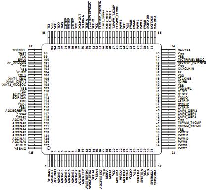
-128-Pin LQFP Without External Memory Interface (PBK) (2810, 2811)
`Temperature Options:
- A: -40 to 85 (GHH, ZHH, PGF, PBK)
- S/Q:-40 to 125 (GHH, ZHH, PGF, PBK)
Pinout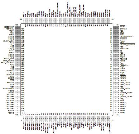
Specifications
| Supply voltage range, VDDIO, VDDA1 , VDDA2 , VDDAIO , and AVDDREFBG |
- 0.3 V to 4.6 V |
| Supply voltage range, VDD, VDD1 |
- 0.5 V to 2.5 V |
| VDD3VFLrange |
- 0.3 V to 4.6 V |
Input voltage range, VIN
|
- 0.3 V to 4.6 V |
| Output voltage range, VO |
- 0.3 V to 4.6 V |
| Input clamp current, IIK(VIN < 0 or VIN > V DDIO )+ |
20 mA |
| Output clamp current, IOK(VO < 0 or VO > VDDIO ) |
20 mA |
Operating ambient temperature ranges, TA:A version (GHH, PGF, PBK)
TA:S version (GHH, PGF, PBK)
TA:Q version (GHH, PGF, PBK) |
-40C to 85
-40C to 125
-40C to 125 |
| Storage temperature range, Tstg+ |
-65C to 150 |
+Continuous clamp current per pin is 2 mA
 Long-term high-temperature storage and/or extended use at maximum temperature conditions may result in a eduction of overall device life. For additional information, see IC Package Thermal Metrics Application Report (literature number SPRA953) and eliability Data for TMS320LF24x and TMS320F281x Devices Application Report (literature number SPRA963).
 Replaced by Q temperature option from silicon revision E onwardsDescription
The TMS320F2810, TMS320F2811, TMS320F2812, TMS320C2810, TMS320C2811, and TMS320C2812 TMS320F2811PBKA devices, members of the TMS320C28x TMS320F2811PBKA DSP generation, are highly integrated, high-performance solutions for demanding control applications. The functional blocks and the memory maps are described in Section 3, Functional Overview.
Throughout this document, TMS320F2810, TMS320F2811, and TMS320F2812 are abbreviated as F2810, F2811, and F2812, TMS320F2811PBKA respectively. F281x denotes all three Flash devices. TMS320C2810, TMS320C2811, and MS320C2812 are abbreviated as C2810, C2811, and C2812, respectively. C281x denotes all three ROM devices. 2810 denotes both F2810 and C2810 devices; 2811 denotes both F2811 and C2811 devices; and 2812 denotes both F2812 and C2812 devices.
Parameters: | Technical/Catalog Information | TMS320F2811PBKA |
| Vendor | Texas Instruments |
| Category | Integrated Circuits (ICs) |
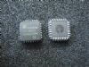
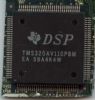
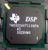
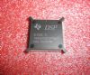
| Package / Case | 128-LQFP |
| Packaging | Tube |
| Type | Fixed Point |
| Non-Volatile Memory | FLASH (256 kB), OTP (2 kB), ROM (8 kB) |
| On-Chip RAM | 36kB |
| Interface | CAN, McBSP, SCI, SPI |
| Voltage - I/O | 3.30V |
| Voltage - Core | 1.90V |
| Clock Rate | 150MHz |
| Operating Temperature | -40°C ~ 85°C |
| Drawing Number | 296; 4040279-3; PBK; 128 |
| Lead Free Status | Lead Free |
| RoHS Status | RoHS Compliant |
| Other Names | TMS320F2811PBKA
TMS320F2811PBKA
296 15988 5 ND
296159885ND
296-15988-5
|

 TMS320F2811PBKA Data Sheet