DescriptionThe TMS320LC549 is a pixed-point digital signal processor fixed-point,it digital signal processor (DSP) (hereafter referred to as the TMS320LC549 is based on an advanced modified Harvard architecture that has one program memory bus and three data memory buses. It also utilizes
a highly specialized instruction set, which is the basis of its operational flexibility and speed.This data sheet contains the pin layouts, signal descriptions, and electrical specifications for the TMS320VC549 DSP.
Features of the TMS320LC549 are:(1)Advanced Multibus Architecture With Three Separate 16-Bit Data Memory Buses and One Program Memory Bus;(2)40-Bit Arithmetic Logic Unit (ALU) Including a 40-Bit Barrel Shifter and Two Independent 40-Bit Accumulators;(3)17-*17-Bit Parallel Multiplier Coupled to a 40-Bit Dedicated Adder for Non-Pipelined Single-Cycle Multiply/Accumulate (MAC) Operation;(4)Compare, Select, and Store Unit (CSSU) for the Add/Compare Selection of the Viterbi Operator;(5)Exponent Encoder to Compute an Exponent Value of a 40-Bit Accumulator Value in a Single Cycle;(6)Two Address Generators With Eight Auxiliary Registers and Two Auxiliary Register Arithmetic Units (ARAUs);(7)Data Bus With a Bus Holder Feature;(8)Address Bus With a Bus Holder Feature;(9)Extended Addressing Mode for 8M*16-Bit Maximum Addressable External Program Space;(10)192K*16-Bit Maximum Addressable
Memory Space (64K Words Program,64K Words Data, and 64K Words I/O);(11)On-Chip ROM with Some Configurable to Program/Data Memory;(12)Dual-Access On-Chip RAM;(13)Single-Access On-Chip RAM;(14)Single-Instruction Repeat and Block-Repeat Operations for Program Code;(15)Block-Memory-Move Instructions for Better Program and Data Management;(16)Instructions With a 32-Bit Long Word Operand;(17)Instructions With Two- or Three-Operand Reads;(18)Arithmetic Instructions With Parallel Store and Parallel Load;(19)Conditional Store Instructions;(20)Fast Return From Interrupt;(21)On-Chip Peripherals:Software-Programmable Wait-State Generator and Programmable Bank SwitchingOn-Chip Phase-Locked Loop (PLL) Clock Generator With Internal Oscillator or External Clock SourceTime-Division Multiplexed (TDM) Serial PortBuffered Serial Port (BSP)8-Bit Parallel Host-Port Interface (HPI)One 16-Bit TimerExternal-Input/Output (XIO) Off Control to Disable the External Data Bus, Address Bus and Control Signals;(22)Power Consumption Control With IDLE1, IDLE2, and IDLE3 Instructions With Power-Down Modes;(23)CLKOUT Off Control to Disable CLKOUT;(24)On-Chip Scan-Based Emulation Logic, IEEE Std 1149.1† (JTAG) Boundary Scan Logic;(25)15-ns Single-Cycle Fixed-Point Instruction Execution Time (66 MIPS) for 3.3-V Power Supply;(26)12.5-ns Single-Cycle Fixed-Point Instruction Execution Time (80 MIPS) for 3.3-V Power Supply.
The absolute maximum ratings of the TMS320LC549 can be summarized as:(1)Supply voltage, DVDD‡:0.3 V to 4.6 V;(2)Input voltage range:0.3 V to 4.6 V;(3)Output voltage range:0.3 V to 4.6 V;(4)Operating case temperature range, TC:40°C to 100°C;(5)Storage temperature range, Tstg:55°C to 150°C. † Stresses beyond those listed under "absolute maximum ratings" may cause permanent damage to the device. These are stress ratings only, and functional operation of the device at these or any other conditions beyond those indicated under "recommended operating conditions" is not implied. Exposure to absolute-maximum-rated conditions for extended periods may affect device reliability.
‡ All voltage values are with respect to VSS.
If you want to know more information such as the electrical characteristics about the TMS320LC549, please download the datasheet in www.seekic.com or www.chinaicmart.com .

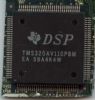
 TMS320LC549 Data Sheet
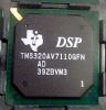