TMU3100

Features: Compliance with the Universal Serial Bus specification v1.1Built-in USB Transceiver and 3.3V regulatorSupport USB Suspend and Resume functionOne Control IN/OUT and two Interrupt IN endpointsPS2 compatible keyboard interface share with USB interface192 byte internal SRAM8K x 14 internal p...

product image

TMU3100 Picture
SeekIC No. : 004525196 Detail

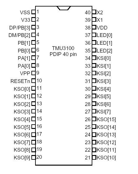
TMU3100: Features: Compliance with the Universal Serial Bus specification v1.1Built-in USB Transceiver and 3.3V regulatorSupport USB Suspend and Resume functionOne Control IN/OUT and two Interrupt IN endpoin...

floor Price/Ceiling Price

Part Number:
TMU3100
Supply Ability:
5000

Price Break

  • Qty
  • 1~5000
  • Unit Price
  • Negotiable
  • Processing time
  • 15 Days
Total Cost: $ 0.00

SeekIC Buyer Protection PLUS - newly updated for 2013!

  • Escrow Protection.
  • Guaranteed refunds.
  • Secure payments.
  • Learn more >>

Month Sales

268 Transactions

Rating

evaluate  (4.8 stars)

Upload time: 2024/4/30

Payment Methods

All payment methods are secure and covered by SeekIC Buyer Protection PLUS.

Notice: When you place an order, your payment is made to SeekIC and not to your seller. SeekIC only pays the seller after confirming you have received your order. We will also never share your payment details with your seller.
Product Details

Description


Features:

Compliance with the Universal Serial Bus specification v1.1
Built-in USB Transceiver and 3.3V regulator
Support USB Suspend and Resume function
One Control IN/OUT and two Interrupt IN endpoints
PS2 compatible keyboard interface share with USB interface
192 byte internal SRAM
8K x 14 internal program OTP-ROM
8-bit RISC CPU core with only 36 instruction
3MHz instruction rate with 6MHz crystal oscillation
40/48 pin package


Pinout

  Connection Diagram


Specifications

Name Symbol Range Range
Maximum Supply Voltage VDD -0.3 to 5.5 V
Maximum Input Voltage Vin -0.3 to VDD+0.3 V
Maximum output Voltage Vout -0.3 to VDD+0.3 V
Maximum Operating Temperature Topg -5 to +70
Maximum Storage Temperature Tstg -25 to +125


Description

TMU3100 1.1 Clock Scheme and Instruction Cycle
The clock input (X1) is internally divided by two to generate Q1 state and Q2 state for each instruction cycle.The Programming Counter (PC) is updated at Q1 and the instruction is fetched from program ROM andlatched into the instruction register in Q2. It is then decoded and executed during the following Q1-Q2 cycle.

1.2 Programming Counter (PC) and Stack
The Programming Counter is 13-bit wide capable of addressing a 8K x 14 program ROM. As a programinstruction is executed, the PC will contain the address of the next program instruction to be executed. ThePC value is normally increased by one except the followings. The Reset Vector (0) and the Interrupt Vector(1) are provided for PC initialization. For CALL/GOTO instructions, PC loads its lower 12 bits from instructionword and the MSB from STATUS's bit 6. For RET/RETI/RETLW instructions, PC retrieves its content fromthe top level STACK. For the other instructions updating PC[7:0], the PC[12:8] keeps unchanged.The STACK is 13-bit wide and 6-level in depth. The CALL instruction and Hardware interrupt will pushSTACK level in order, While the RET/RETI/RETLW instruction pops the STACK level in order.

1.3 Addressing Mode
There are two Data Memory Plane in CPU, R-Plane and F-Plane. The registers in R-Plane are write-only.The "MOVWR" instruction copy the W-register's content to those registers by direct addressing mode.Registers in F-Plane can be addressed directly or indirectly. Indirect Addressing is made by address "0",where FSR points to an actual address. The first half of F-Plane is also bit-addressable.


Customers Who Bought This Item Also Bought

Margin,quality,low-cost products with low minimum orders. Secure your online payments with SeekIC Buyer Protection.
Discrete Semiconductor Products
Soldering, Desoldering, Rework Products
Power Supplies - External/Internal (Off-Board)
Prototyping Products
DE1
Memory Cards, Modules
View more