TNETA1500

Features: ` Single-Chip Receiver/Transmitter for Transporting 53-Byte ATM Cells Via STS-3c/STM-1 Frame (155.52 Mbit/s)` On-Chip Analog Phase-Locked Loop (APLL) Provides: Recovery of Receive Clock From Incoming Serial-Data Stream Transmit Clock Generation From External 19.44-MHz Clock Source` Ins...

product image

TNETA1500 Picture
SeekIC No. : 004525450 Detail

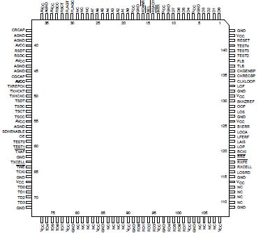
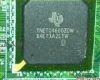
TNETA1500: Features: ` Single-Chip Receiver/Transmitter for Transporting 53-Byte ATM Cells Via STS-3c/STM-1 Frame (155.52 Mbit/s)` On-Chip Analog Phase-Locked Loop (APLL) Provides: Recovery of Receive Clock F...

floor Price/Ceiling Price
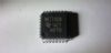
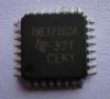
Part Number:
TNETA1500
Supply Ability:
5000

Price Break

  • Qty
  • 1~5000
  • Unit Price
  • Negotiable
  • Processing time
  • 15 Days
Total Cost: $ 0.00

SeekIC Buyer Protection PLUS - newly updated for 2013!

  • Escrow Protection.
  • Guaranteed refunds.
  • Secure payments.
  • Learn more >>

Month Sales

268 Transactions

Rating

evaluate  (4.8 stars)

Upload time: 2024/4/27

Payment Methods

All payment methods are secure and covered by SeekIC Buyer Protection PLUS.

Notice: When you place an order, your payment is made to SeekIC and not to your seller. SeekIC only pays the seller after confirming you have received your order. We will also never share your payment details with your seller.
Product Details

Description


Features:

` Single-Chip Receiver/Transmitter for Transporting 53-Byte ATM Cells Via STS-3c/STM-1 Frame (155.52 Mbit/s)
` On-Chip Analog Phase-Locked Loop (APLL) Provides:
   Recovery of Receive Clock From Incoming Serial-Data Stream
   Transmit Clock Generation From External 19.44-MHz Clock Source
` Inserts and Extracts ATM Cells Into/From SONET/SDH STS-3c/STM-1 SPE
` Detects Multiple-Bit Errors and Corrects Single-Bit Errors in the 5-Byte ATM
  Headers of Incoming ATM Cells
` Generates Alarms for:
   Loss of Incoming Serial Signal (LOS)
   Out of Frame (OOF)
   Loss of Frame (LOF)
   B1-Byte Parity Error (B1ERR)
   Loss of ATM Cell Alignment (LOCA)
   Line Far-End Receive Failure (LFERF)
   Receive Loss of Pointer (LOP)
   Line Alarm Indication Signal (LAIS)
` Meets ATM Forum ATM User-Network
  Interface Specification Requirement
` BiCMOS Device Packaged in 144-Pin Plastic Quad Flat Package (PQFP)


Pinout

  Connection Diagram


Specifications

Supply voltage range, TTL, VCC (see Note 1) . . . . . . . . . . . . .   0.5 V to 7 V
Supply voltage range, PECL, VCC (see Note 1) . . . . . . . . . . . . . 0.5 V to 7 V
Supply voltage range, analog, AVCC (see Note 1) . . . . .  . . . . . 0.5 V to 7 V
Input voltage range:TTL . . . . . . . . . . . . . . . . . . . . . . . . . . . . . . 1.2 V to 7 V
                                 PECL . . . . . . . . . . . . . . . . . . . . . . . . . . .  . . 0 V to PVCC
Operating free-air temperature range, TA . . . . . . . . . . . . . . . . . 0°C to 70°C
Storage temperature range, Tstg . . . . . . . . . . . . . . . . . . .  . 65°C to 150°C

† Stresses beyond those listed under "absolute maximum ratings" may cause permanent damage to the device. These are stress ratings only, and functional operation of the device at these or any other conditions beyond those indicated in the "recommended operating conditions" is not implied. Exposure to absolute-maximum-rated conditions for extended periods may affect device reliability.

NOTE 1: All voltage values are with respect to the GND terminals.


Description

The synchronous optical network (SONET)/synchronous digital hierarchy (SDH) asynchronous transport mode (ATM) line-interface receiver/transmitter provides a single-chip implementation for transporting ATM cells over the SONET/SDH network at the STS-3c/STM-1 rate of 155.52 Mbit/s. This TNETA1500 device provides all the functionality required to insert and extract 53-byte ATM cells into/from a STS-3c/STM-1 synchronous payloadenvelope (SPE), including clock recovery and clock generation using analog phase-locked loops (APLL).

On the receive side, the TNETA1500 accepts 155.52-Mbit/s serial data, recovers the embedded clock signal, performs SONET/SDH frame alignment and serial-to-parallel conversion, identifies the SONET/SDH payload, and establishes the ATM-cell boundaries. The ATM cells are extracted from the payload, descrambled, and passed to the receive output FIFO for output to the next device (i.e., a reassembly device). On the transmit side, complete 53-byte ATM cells are placed into the transmit input FIFO, scrambled, and inserted into an STS-3c/STM-1 SPE. The SONET/SDH frame is scrambled and converted to a serial-data stream for output. An APLL is used to generate the 155.52-MHz output clock from a low-speed 19.44-MHz oscillator, eliminating the need for a high-speed 155.52-MHz oscillator.


Customers Who Bought This Item Also Bought

Margin,quality,low-cost products with low minimum orders. Secure your online payments with SeekIC Buyer Protection.
Circuit Protection
RF and RFID
Hardware, Fasteners, Accessories
Cables, Wires - Management
Optical Inspection Equipment
View more