Features: ` Dual Output Voltages for Split-Supply pplications
` electable Power Up Sequencing for DSP pplications
` Output Current Range of 500 mA on egulator 1 and 250 mA on Regulator 2
` Fast Transient Response
` oltage Options are 3.3-V/2.5-V, 3.3-V/1.8-V, .3-V/1.5-V, 3.3-V/1.2-V, and Dual Adjustable utputs
` Open Drain Power-On Reset With 120-ms elay
` Open Drain Power Good for Regulator 1
` Ultra Low 190 mA (typ) Quiescent Current
` 1 A Input Current During Standby
` Low Noise: 65 VRMS Without Bypass apacitor
` Quick Output Capacitor Discharge Feature
` Two Manual Reset Inputs
` 2% Accuracy Over Load and Temperature
` Undervoltage Lockout (UVLO) Feature
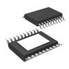
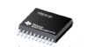
` 20-Pin PowerPAD™ TSSOP Package
` Thermal Shutdown ProtectiPinout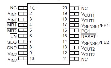 Specifications
Input voltage range‡: VIN1 . . . . . . . . . . . . . . . . . . . . . . . 0.3 V to 7 V
VIN2 . . . . . . . . . . . . . . . . . . . . . . . . . . . . . . . . . . . . . . . . . 0.3 V to 7 V
Voltage range at EN . . . . . . . . . . . . . . . . . . . . . . . . . . . . 0.3 V to 7 V
Output voltage range (VOUT1, VSENSE1) . . . . . . . . . . . . . . . . . . . .. 5.5 V
Output voltage range (VOUT2, VSENSE2) . . . . . . . .. . . . . . . . . . . . . 5.5 V
Maximum RESET, PG1 voltage . . . . . . . . . . . . . . . . . . . . . .. . . . . . . . 7 V
Maximum MR1, MR2, and SEQ voltage . . . . . . . . . . . . . . . . . . .. . . . VIN1
Peak output current . . . . . . . . . . . . . . . . . . . . . . . . . . Internally limited
Continuous total power dissipation . . . . See Dissipation Rating Tables
Operating virtual junction temperature range, TJ . . .. . . 40 to 125
Storage temperature range, Tstg . . . . . . . . . . . . . . . . . .65 to 150
ESD rating, HBM . . . . . . . . . . . . . . . . . . . . . . . . . . . . . . . . . . . .. . . . 2 kV
† Stresses beyond those listed under "absolute maximum ratings" may cause permanent damage to the device. These are stress ratings only, and unctional operation of the device at these or any other conditions beyond those indicated under "recommended operating conditions" is not mplied. Exposure to absolute-maximum-rated conditions for extended periods may affect device reliability.
‡ All voltages are tied to network ground.
DescriptionTPS701xx family devices are designed to provide complete power management solution for DSP, rocessor power, ASIC, FPGA, and digital pplications where dual output voltage regulators re required. Easy programmability of the equencing function makes TPS701xx family ideal for ny DSP applications with power sequencing equirement. Differentiated features, such as ccuracy, fast transient response, SVS supervisory ircuit, manual reset inputs, and enable unction, provide a complete system solution.
The TPS701xx family of voltage regulators offers very low dropout voltage and dual outputs with power up
sequence control, which is designed primarily for DSP applications. TPS701xx family have extremely low noise
output performance without using any added filter bypass capacitors and are designed to have a fast transient
response and be stable with 10 uF low ESR capacitors.
TPS701xx family has fixed 3.3-V/2.5-V, 3.3-V/1.8-V, 3.3-V/1.5-V, 3.3-V/1.2-V, and adjustable/adjustable voltage ptions. The 3.3-V output regulator (regulator 1) can support up to 500 mA, and the other regulator (regulator ) can support up to 250 mA. Separate voltage inputs allow the designer to configure the source power.
ecause the PMOS TPS701xx family behaves as a low-value resistor, the dropout voltage is very low (typically 170 mV n regulator 1) and is directly proportional to the output current. Additionally, since the PMOS pass element is voltage-driven device, the quiescent current is very low and independent of output loading (maximum of 225 A over the full range of output current). This LDO TPS701xx family also features a sleep mode; applying a high signal to EN (enable) shuts down both regulators, reducing the input current to 1 A at TJ = 25°C.
The TPS701xx family is enabled when the EN pin is connected to a low-level input voltage. The output voltages of the two egulators are sensed at the VSENSE1 and VSENSE2 pins respectively. The input signal at the SEQ pin controls he power-up sequence of the two regulators. When the TPS701xx family is enabled and the SEQ terminal is pulled high r left open, VOUT2 will turn on first and VOUT1 will remain off until VOUT2 reaches approximately 83% of it's egulated output voltage. At that time VOUT1 will be turned on. If VOUT2 is pulled below 83% (i.e. over load ondition) VOUT1 will be turned off. Pulling the SEQ terminal low, reverses the power-up order and VOUT1 will e turned on first. The SEQ pin is connected to an internal pullup current source.
For each regulator, there is an internal discharge transistor to discharge the output capacitor when the regulator
is turned off(disabled).
The PG1 pin of TPS701xx family reports the voltage conditions at the VOUT1, which can be used to implement a SVS (power on eset) for the circuitry supplied by regulator 1.
The TPS701xx features a RESET (SVS, POR, or Power On Reset). RESET output initiates a reset in DSP ystems in the event of an undervoltage condition. RESET indicates the status of the VOUT2 and both manual eset pins ( MR1 and MR2). When VOUT2 reaches 95% of it's regulated voltage and MR1 andMR2 are in the ogic high state, RESETwill go to a high impedance state after 120 ms delay. RESET will go to logic low state hen VOUT2 regulated output voltage of TPS701xx family is pulled below 95% (i.e. over load condition) of it's regulated voltage. To onitor VOUT1 , the PG1 output pin can be connected to MR1 or MR2.
The TPS701xx family have an undervoltage lockout UVLO circuit which prevents the internal regulators from turning on until IN1 reaches 2.5V.

 TPS70145 Data Sheet