Features: · Charge Pump Provides Negative Gate Bias for Depletion-Mode GaAs Power Amplifiers
· Buffered Clock Output to Drive Additional External Charge Pump
·135-mW High-Side Switch Controls Supply Voltage to the GaAs Power Amplifier
· Power-Good Circuitry Prevents High-Side Switch Turn-on Until Negative Gate Bias is Present
· Charge Pump Can Be Driven From the Internal Oscillator or An External Clock
·10-mA Maximum Standby Current
·Low-Profile (1.2-mm Max Height), 20-Pin TSSOP Package
Pinout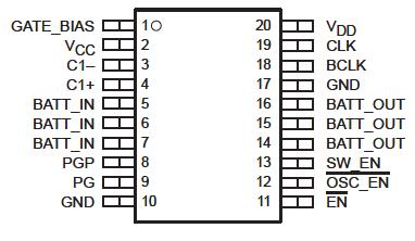 Specifications
High-side switch input voltage range, BATT_IN (see Note 1) . . . . . . . . . . . . . . . . . . . . . . . . . . . . 0.3 V to 15 V
Supply voltage range, VCC, VDD . . . . . . . . . . . . . . . . . . . . . . . . . . . . . . . . . . . . . . . . . . . . . . . . . . . . . 0.3 V to 7 V
Differential voltage, |BATT_IN||GATE_BIAS| . . . . . . . . . . . . . . . . . . . . . . . . . . . . . . . . . . . . . . . . . . . . . . . . . 15 V
Input voltage range, SW_EN, EN, CLK, OSC_EN, PG . . . . . . . . . . . . . . . . . . . . . . . . . . 0.3 V to VCC + 0.3 V
GATE_BIAS . . . . . . . . . . . . . . . . . . . . . . . . . . . . . . . . . . . . . . . . . . . . . . . . . . . . . . . . . . . . . . . . . . . . . . . . . . . . 5.5 V
Output current, PG . . . . . . . . . . . . . . . . . . . . . . . . . . . . . . . . . . . . . . . . . . . . . . . . . . . . . . . . . . . . . . . . . . . . . . . . 5 mA
Output current, BCLK . . . . . . . . . . . . . . . . . . . . . . . . . . . . . . . . . . . . . . . . . . . . . . . . . . . . . . . . . . . . . . . . . . . . . 50 mA
Output current, GATE_BIAS . . . . . . . . . . . . . . . . . . . . . . . . . . . . . . . . . . . . . . . . . . . . . . . . . . . . . . . . . . . . . . . 10 mA
Output current, BATT_OUT . . . . . . . . . . . . . . . . . . . . . . . . . . . . . . . . . . . . . . . . . . . . . . . . . . . . . . . . . . . . . . . . . 2 A
Peak output current, BATT_OUT . . . . . . . . . . . . . . . . . . . . . . . . . . . . . . . . . . . . . . . . . . . . . . . . . . . . . . . . . . . . . 4 A
Maximum external clock frequency, CLK . . . . . . . . . . . . . . . . . . . . . . . . . . . . . . . . . . . . . . . . . . . . . . . . . . 100 kHz
Continuous total power dissipation . . . . . . . . . . . . . . . . . . . . . . . . . . . . . . . . . . . . . See Dissipation Rating Table
Junction temperature range, TJ . . . . . . . . . . . . . . . . . . . . . . . . . . . . . . . . . . . . . . . . . . . . . . . . . . . 25°C to 150°C
Storage temperature range, Tstg . . . . . . . . . . . . . . . . . . . . . . . . . . . . . . . . . . . . . . . . . . . . . . . . . . 65°C to 150°C
† Stresses beyond those listed under "absolute maximum ratings" may cause permanent damage to the device. These are stress ratings only, and functional operation of the device at these or any other conditions beyond those indicated under "recommended operating conditions" is not implied. Exposure to absolute-maximum-rated conditions for extended periods may affect device reliability.
NOTES:
1. All voltages are with respect to device GND.
2. Differential voltage calculated: |VImax| + |GATE_BIAS|
DescriptionThe TPS9103 is a highly integrated power supply for depletion-mode GaAs power amplifiers (PA) in cellular handsets and other wireless communications equipment. Functional integration and low-profile packaging combine to minimize circuit-board area and component height requirements. The TPS9103e includes: a p-channel MOSFET configured as a high-side switch to control the application of power to the PA; a driver for the high-side switch with a logic-compatible input; a charge pump to provide negative gate-bias voltage; and logic to prevent turn-on of the high-side switch until gate bias is present. The high-side switch of TPS9103 has a typical on-state resistance of 135 mW.
The TPS9103 is available in a 20-pin thin shrink small-outline package (TSSOP) or in chip form. Contact factory for die sales. The device operates over a junction temperature range of 25°C to 125°C.

 TPS9103 Data Sheet