Features: Link
• Supports Provision of IEEE 1394-1995 (1394) Standard for High-Performance Serial Bus
• Transmits and Receives Correctly Formatted 1394 Packets
• Supports Isochronous Data Transfer
• Performs Function of 1394 Cycle Master
• Generates and Checks 32-Bit CRC
• Detects Lost Cycle-Start Messages
• Contains Asynchronous, Isochronous, and General-Receive FIFOs Totaling 2K Bytes
Physical-Link Interface
• Interfaces Directly to the TSB11LV01, TSB14C01, TSB21LV03A, and TSB41LV0x PHY Chips
• Supports Speeds of 100 Mbits/s, 200 Mbits/s, and 400 Mbits/s
• Implements the Physical-Link Interface Described in Annex J of the IEEE 1394-1995 Standard
• Supports TI Bus Holder Isolation External Implementation
Host Bus Interface
• Provides Chip Control With Directly Addressable Registers
• Is Interrupt Driven to Minimize Host Polling
• Has a Generic 32-Bit Host Bus Interface General
• Operates from a 3.3-V Power Supply While Maintaining 5-V Tolerant Inputs
• Manufactured with Low-Power CMOS Technology
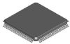
• Packaged in a 100-Pin Thin Quad Flat Package (TQFP) (PZ Package) for 0°C to 70°C and 40°C to 85°C Operation
Pinout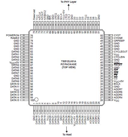 SpecificationsSupply voltage range, VCC . . . . . . . . . . . . . . . . . . . . . . . . . . . . . . . . .0.5 V to 3.6 V
Supply voltage range, VCC5V . . . . . . . . . . . . . . . . . . . . . . . . . . . . . . . 0.5 V to 5.5 V
Input voltage range, VI (standard TTL/LVCMOS) . . . . . . . . . . . .0.5 V to VCC + 0.5 V
Input voltage range, VI (5-V standard TTL/LVCMOS) . . . . . . . . .0.5 V to VCC + 0.5 V
Output voltage range, (standard TTL/LVCMOS) VO . . . . . . . . . . 0.5 V to VCC + 0.5 V
Output voltage range, (5-V standard TTL/LVCMOS) VO . . . . . . . 0.5 V to VCC + 0.5 V
Input clamp current, IIK (TTL/LVCMOS) (VI < 0 or VI > VCC) (see Note 1) . . . .. ±20 mA
Output clamp current, IOK (TTL/LVCMOS) (VO < 0 or VO > VCC) (see Note 2) . .±20 mA
Continuous total power dissipation . . . . . . . . . . See Maximum Dissipation Rating Table
Operating free-air temperature range, TA (TSB12LV01A) . . . . . . . . . . . . .0°C to 70°C
Operating free-air temperature range, (TSB12LV01AI) . . . . . . . . . . . 40°C to 85°C
Storage temperature range, Tstg . . . . . . . . . . . . . . . . . . . . . . . . . .. . 65°C to 150°C
NOTES:
1. This applies to external input and bidirectional buffers. For 5-V tolerant terminals, use VI > VCC5V.
2. This applies to external output and bidirectional buffers. For 5-V tolerant terminals, use VO > VCC5V.DescriptionThe TSB12LV01A is an IEEE 1394-1995 standard (from now on referred to only as 1394) high-speed serial-bus link-layer controller that allows for easy integration into an I/O subsystem. The TSB12LV01 A provides a high-performance IEEE 1394-1995 interface with the capability of transferring data between the 32-bit host bus, the 1394 PHY-link interface, and external devices connected to the local bus interface. The 1394 PHY-link interface provides the connection to the 1394 physical (PHY) layer device and is supported by the link-layer controller (LLC). The LLC provides the control for transmitting and receiving 1394 packet data between the FIFO and PHY-link interface at rates of 100Mbit/s, 200Mbit/s, and 400Mbit/s. The TSB12LV01A transmits and receives correctly-formatted 1394 packets and generates and inspects the 32-bit cyclic redundancy check (CRC). The TSB12LV01 A is capable of being cycle master and supports reception of isochronous data on two channels or all isochronous channels. TSB12LV01A has a generic 32-bit host bus interface, which connects to most 32-bit hosts. The LLC also provides the capability to receive status from the physical layer device and to access the physical layer control and status registers by the application software. An internal 2K-byte memory can be configured as multiple variable-size FIFOs and eliminates the need for external FIFOs. Separate FIFOs can be user-configured to support general 1394 receive, asynchronous transmit, and isochronous transmit transfer operations. These functions are accomplished by appropriately sizing the general receive FIFO (GRF), asynchronous transmit FIFO (ATF), and isochronous transmit FIFO (ITF).
The TSB12LV01A provides bus holding buffers on the PHY interface for simple and cost effective single-capacitor isolation. The TSB12LV01 A is a revision of the TSB12C01A, with feature enhancements and corrections. All errata items to the TSB12C01A have been corrected, and the following feature enhancements have been made:
• Cycle start packets can be stored in the GRF.
• Isochronous and asynchronous packet transmit and receive can be enabled/disabled independently. Asynchronous transmit is disabled upon reset, while isochronous transmit and receive is unaffected.
• One, two, or all isochronous channels can be received.
• When receiving packets, RxDta can be programmed to interrupt the host processor on programmable block boundaries, so the host can retrieve data from the GRF when each block is available. This is especially useful if the GRF is smaller than the expected receive packet size. RxDta can also be programmed to interrupt the host processor when each packet is received.
• Host bus burst mode data transfer is supported, at the peak rate of one quadlet (four bytes) per BClk cycle for ATF write, ITF write, and GRF read.
• A FIFO status read can be accomplished in three BClk cycles: 1. Address cycle 2. Data cycle 3. Idle cycle
• Several changes in the register map have been made to improve host bus data throughput and reduce status read and interrupt overhead. ATF status (30h), ITF status (34h) and GRF status (3Ch) contains only status information. FIFO control (1Ch) is defined to control ATF size, ITF size, clear FIFO function, and block size for GRF received packet. ATF status register and ITF status register will report flags: full, empty and available space for host bus burst write. GRF status register will report flags: empty, total stored data count, and next received block size.
• Maximum data burst throughput on the host bus interface is 200 Mbyte/s, if Bclk is run at 50 MHz.
• Received packet formats now include the packet error status in the first quadlet of the packet in the receive FIFO.
• Provides bus-hold buffers on physical interface for low-cost single capacitor isolation This document is not intended to serve as a tutorial on 1394; users are referred to the IEEE 1394-1995 serial bus standard for detailed information regarding the 1394 high-speed serial bus.

 TSB12LV01A Data Sheet