Features: · Supports Provisions of IEEE 1394-1995 (1394) Standard for High-Performance Serial Bus†
· Performs the Function of a 1394 Cycle Master
· Supports 1394 Transfer Rates of 100, 200 and 400 Mbit/s
· Provides Three Sizes of Programmable FIFOs
· Provides PCI Bus Master Function for Supporting DMA Operations
· Compliant With PCI Specification 2.1
· Provides PCI Slave Function for Read/Write Access of Internal Registers
· Supports the Plug-and-Play (PnP) Specification
· Provides an 8-/16-bit Zoom Video (ZV) Port for the Transferring of Video Data Directly to an External Motion Video Memory Area
· Operates from a 3.3-V Power Supply While Maintaining 5-V Tolerant Inputs
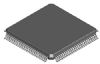
· High-Performance 176-Pin PQFP (PGF) Package
Pinout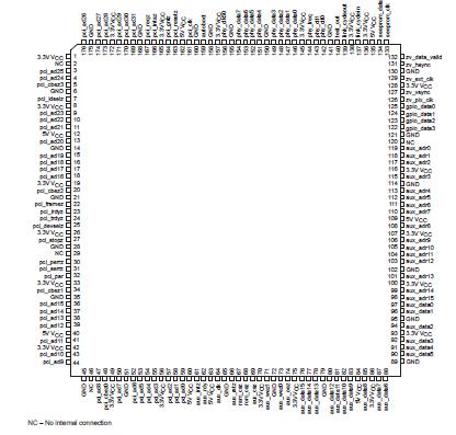 SpecificationsSupply voltage range, VCC(3V) (VCC = 3 V) . . . . . . . . . . . . 0.5 V to 4.0 V
Supply voltage range, VCC(5V) (VCC = 5 V) . . . . . . . . . . . . . 0.5 V to 5.5 V
Input voltage range, VI . . . . . . . . . . . . . . . . . . . .. 0.5 V to VCC(5v) +0.5 V
Output voltage range at any output, VO . . . . . . . 0.5 V to VCC(5v) + 0.5 V
Input clamp current, IIK (VI < 0 or VI > VCC5) . . . . . . . . . . . . . . . .. ± 20 mA
Storage temperature range, Tstg . . . . . . . . . . . . . . . . . . .65°C to 150°C
† Stresses beyond those listed under "absolute maximum ratings" may cause permanent damage to the device. These are stress ratings only, and functional operation of the device at these or any other conditions beyond those indicated under "recommended operating conditions" is not implied. Exposure to absolute-maximum-rated conditions for extended periods may affect device reliability.DescriptionThe TSB12LV21A (PCILynx) provides a high-performance IEEE 1394-1995 interface with the capability to transfer data between the 1394 phy-link interface, the PCI bus interface, and external devices connected to the local bus interface. The 1394 phy-link interface provides the connection to the 1394 physical layer device and is supported by the on-board link layer controller (LLC). The LLC provides the control for transmitting and receiving 1394 packet data between the FIFO and phy-link interface at rates of 100 Mbit/s, 200 Mbit/s, and 400 Mbit/s. The link layer also provides the capability to receive status from the physical layer device and to access the physical layer control and status registers by the application software.
An internal 1K-byte memory is provided that can be configured as multiple variable-size FIFOs and eliminates the need for external FIFOs. Separate FIFOs can be user configured to support 1394 receive, asynchronous transmit, and isochronous transmit transfer operations.
The PCI interface supports 32-bit burst transfers up to 33 MHz and is capable of operating as both master and target devices. Configuration registers can be loaded from an external serial EEPROM, allowing board and system designers to assign their own unique identification codes. An autoboot mode allows data-moving systems (such as docking stations) to be designed to operate on the PCI bus without the need for a host CPU.
The DMA controller uses packet control list (PCL) data structures to control the transfer of data and allow the
DMA to operate without host CPU intervention. These PCLs can reside in PCI memory or in memory that is connected to the local bus port. The PCLs implement an instruction set that allows linking, conditional branching, 1394 data transfer control, auxiliary support commands, and status reporting. Five DMA channels are provided to accommodate programmable data types. PCLs can be chained together to form a channel control program that can be developed to support each DMA channel. Data can be stored in either big endian or little endian format eliminating the need for the host CPU to perform byte swapping. Data can be transferred to either 4-byte aligned locations to provide the highest performance or to nonaligned locations to provide the best memory use.
The RAM, ROM, AUX, ZV, and general purpose I/O (GPIO) ports collectively implement the local bus interface. These ports are mapped into the PCI address can be accessed either through the PCI bus or internal DMA transactions. Internal transactions do not appear on the external PCI bus, thereby conserving PCI bandwidth. DMA packet control lists or other data that may be stored in external RAM or ROM attached to the local bus interface. This further reduces PCI use and generally improves performance. The ZV local bus port is designed to transfer data from 1394 video devices to an external device connected to the PCILynx ZV port. This interface provides a method of receiving 1394 digital camera packets directly to a ZV-compliant device attached to the local bus interface.
Built-in test registers, a dedicated test output terminal, and four GPIO terminals allow observation of internal states and provides a convenient software debug capability. Programmable interrupts are available to inform driver software of important events such as 1394 bus resets and DMA-to-PCL transfer completion. The 3.3-V internal operation provides reduced power consumption while maintaining compatibility with 5-V signaling environments. The PCI interface is compatible with both 3-V and 5-V PCI systems.

 TSB12LV21 Data Sheet