Features: · Fully Supports Provisions of IEEE 1394-1995 Standard for High Performance Serial Bus† and IEEE 1394a-2000
· Fully Interoperable With FireWire and i.LINK Implementation of IEEE Std 1394
· Fully Compliant With OpenHCI Requirements
· Provides One IEEE 1394a-2000 Fully Compliant Cable Port at 100/200/400 Megabits Per Second (Mbits/s)
· Full IEEE 1394a-2000 Support Includes: Connection Debounce, Arbitrated Short Reset, Multispeed Concatenation, Arbitration Acceleration, Fly-By Concatenation, Port Disable/Suspend/Resume
· Register Bits Give Software Control of Contender Bit, Power Class Bits, Link Active Control Bit, and IEEE 1394a-2000 Features
· IEEE 1394a-2000 Compliant Common Mode Noise Filter on Incoming TPBIAS
· Extended Resume Signaling for Compatibility With Legacy DV Devices, and Terminal- and Register-Compatibility With TSB41LV01, Allow Direct Isochronous Transmit to Legacy DV Devices With Any Link Layer Even When Root
· Power-Down Features to Conserve Energy in Battery Powered Applications Include: Automatic Device Power Down During Suspend, Device Power-Down Terminal, Link Interface Disable via LPS, and Inactive Ports Powered Down
· Failsafe Circuitry Senses Sudden Loss of Power to the Device and Disables the Port to Ensure That the Device Does Not Load TPBIAS of the Connected Device and Blocks Any Leakage Path From the Port Back to the Device Power Plane · Software Device Reset (SWR)
· Industry Leading Low Power Consumption
· Ultralow-Power Sleep Mode
· Cable Power Presence Monitoring
· Cable Ports Monitor Line Conditions for Active Connection to Remote Node
· Data Interface to Link-Layer Controller Through 2/4/8 Parallel Lines at 49.152 MHz
· Interface to Link Layer Controller Supports Low Cost TI Bus-Holder Isolation and Optional Annex J Electrical Isolation
· Interoperable With Link-Layer Controllers Using 3.3 V
· Single 3.3-V Supply Operation
· Low-Cost 24.576-MHz Crystal Provides Transmit, Receive Data at 100/200/400 Mbits/s, and Link-Layer Controller Clock at 49.152 MHz
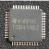
· Low-Cost High-Performance 48/64-Pin TQFP (PHP/PAP) Thermally Enhanced Packages Increase Thermal Performance by up to 210%
· Meets Intel Mobile Power Guideline 2000
· Available in MicroStar Junior BGA (GQE) Package
Pinout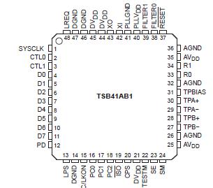
SpecificationsSupply voltage range, VDD (see Note 1) . . . . . . . . . . . . . . . . . . . . . . . . −0.3 V to 4 V
Input voltage range, VI . . . . . . . . . . . . . . . . . . . . . . . . . . . . . . −0.5 V to VDD + 0.5 V
Output voltage range at any output, VO . . . . . . . . . . . . . . . . . .−0.5 V to VDD + 0.5V
Continuous total power dissipation . . . . . . . . . . . . . . . See Dissipation Rating Table
Operating free air temperature, TA . . . . . . . . . . . . . . . . . . . . . . . . . . . 0°C to 70°C
Storage temperature range, Tstg . . . . . . . . . . . . . . . . . . . . . . . . . −65°C to 150°C
Lead temperature 1,6 mm (1/16 inch) from case for 10 seconds . . . . . . . . . . 260°C
NOTES:
1. All voltage values, except differential I/O bus voltages, are with respect to network ground.DescriptionThe TSB41AB1 provides the digital and analog transceiver functions needed to implement a one-port node in a cable-based IEEE 1394 network. The cable port incorporates one differential line transceiver. The transceiver includes circuitry to monitor the line conditions as needed for determining connection status, for initialization and arbitration, and for packet reception and transmission. The TSB41AB1 is designed to interface with a link layer controller (LLC), such as the TSB12LV21, TSB12LV22, TSB12LV23, TSB12LV26, TSB12LV31, TSB12LV41, TSB12LV42, or TSB12LV01A.
The TSB41AB1 requires only an external 24.576-MHz crystal as a reference. An external clock may be provided instead of a crystal. An internal oscillator drives an internal phase-locked loop (PLL), which generates the required 393.216-MHz reference signal. This reference signal is internally divided to provide the clock signals used to control transmission of the outbound encoded strobe and data information. A 49.152-MHz clock signal is supplied to the associated LLC for synchronization of the two chips and is used for resynchronization of the received data. The power-down (PD) function, when enabled by asserting the PD terminal high, stops operation of the PLL.
The TSB41AB1 supports an optional isolation barrier between itself and its LLC. When the ISO input terminal is tied high, the LLC interface outputs behave normally. When the ISO terminal is tied low, internal differentiating logic is enabled, and the outputs are driven such that they can be coupled through a capacitive or transformer galvanic isolation barrier as described in Annex J of IEEE Std 1394-1995 and in IEEE 1394a-2000 (section 5.9.4) (hereinafter referred to as Annex J type isolation). To operate with TI bus holder isolation the ISO terminal on the PHY must be high.
Data bits to be transmitted through the cable port are received from the LLC on two, four or eight parallel paths (depending on the requested transmission speed) and are latched internally in the TSB41AB1 in synchronization with the 49.152-MHz system clock. These bits are combined serially, encoded, and transmitted at 98.304, 196.608, or 393.216 Mbits/s (referred to as S100, S200, and S400 speeds, respectively) as the outbound data-strobe information stream. During transmission, the encoded data information is transmitted differentially on the TPB cable pair, and the encoded strobe information is transmitted differentially on the TPA cable pair.
During packet reception the TPA and TPB transmitters of the receiving cable port are disabled, and the receivers for that port are enabled. The encoded data information is received on the TPA cable pair, and the encoded strobe information is received on the TPB cable pair. The received data-strobe information is decoded to recover the receive clock signal and the serial data bits. The serial data bits are split into two-, four-, or eight-bit parallel streams (depending upon the indicated receive speed), resynchronized to the local 49.152-MHz system clock and sent to the associated LLC.
Both the TPA and TPB cable interfaces incorporate differential comparators to monitor the line states during initialization and arbitration. The outputs of these comparators are used by the internal logic to determine the arbitration status. The TPA channel monitors the incoming cable common-mode voltage. The value of this common-mode voltage is used during arbitration to set the speed of the next packet transmission. In addition, the TPB channel monitors the incoming cable common-mode voltage on the TPB pair for the presence of the remotely supplied twisted-pair bias voltage.
The TSB41AB1 provides a 1.86-V nominal bias voltage at the TPBIAS terminal for port termination. This bias voltage, when seen through a cable by a remote receiver, indicates the presence of an active connection. This bias voltage source must be stabilized by an external filter capacitor of 1 F. TPBIAS is typically VDD−0.2 V when the port is not connected to another node.
The line drivers in the TSB41AB1 operate in a high-impedance current mode, and are designed to work with external 112- line-termination resistor networks in order to match the 110- cable impedance. One network is provided at each end of a twisted-pair cable. Each network is composed of a pair of series-connected 56- resistors. The idpoint of the pair of resistors that is directly connected to the twisted-pair-A terminals is connected to its corresponding TPBIAS voltage terminal. The midpoint of the pair of resistors that is directly connected to the twisted-pair-B terminals is coupled to ground through a parallel R-C network with recommended values of 5 k and 220 pF. The values of the external line termination resistors are designed to meet IEEE Std 1394-1995 when connected in parallel with the internal receiver circuits. An external resistor connected between the R0 and R1 terminals sets the driver output current, along with other internal operating currents. This current-setting resistor has a value of 6.34 k ±1.0%.
When the power supply of the TSB41AB1 is off while the twisted-pair cables are connected, the TSB41AB1 transmitter and receiver circuitry presents a high impedance to the cable and does not load the TPBIAS voltage at the other end of the cable. Fail-safe circuitry blocks any leakage path from the port back to the device power plane.
The TESTM, SE, and SM terminals are used to set up various manufacturing test conditions. For normal operation, the TESTM terminal should be connected to VDDthrough a 1-k resistor, SE should be tied to ground through a 1-k resistor, and SM should be connected directly to ground.
Four package terminals are used as inputs to set the default value for four configuration status bits in the self-ID packet, and are tied high through a 1-k resistor or hardwired low as a function of the equipment design. The PC0PC2 terminals are used to indicate the default power-class status for the node (the need for power from the cable or the ability to supply power to the cable). See Table 9 for power-class encoding. The C/LKON terminal is used as an input to indicate that the node is a contender for either isochronous resource manager (IRM) or for bus manager (BM).
The TSB41AB1 supports suspend/resume as defined in the IEEE 1394a-2000 specification. The suspend mechanism allows pairs of directly connected ports to be placed into a low-power state (suspended state) while maintaining a port-to-port connection between bus segments. While in the suspended state, a port is unable to transmit or receive data transaction packets. However, a port in the suspended state is capable of detecting connection status changes and detecting incoming TPBIAS. When the port of the TSB41AB1 is suspended, all circuits except the band gap reference generator and bias detection circuit is powered down, resulting in significant power savings. For additional details of suspend/resume operation see IEEE 1394a-2000. The use of suspend/resume is recommended for new designs.
The port transmitter and receiver circuitry is disabled during power down (when the PD input terminal is asserted
high), during reset (when the RESET input terminal is asserted low), when no active cable is connected to the port, or when controlled by the internal arbitration logic. The TPBIAS output is disabled during power down, during reset, or when the port is disabled as commanded by the LLC.
The cable-not-active (CNA) output terminal (64-terminal PAP package only) is asserted high when there are no twisted-pair cable ports receiving incoming bias (that is, they are either disconnected or suspended), and can be used along with LPS to determine when to power down the TSB41AB1. The CNA output is not debounced. When the PD terminal is asserted high, the CNA detection circuitry is enabled (regardless of the previous state of the ports) and a pulldown is activated on the RESET terminal so as to force a reset of the TSB41AB1 internal logic.
The LPS (link power status) terminal works with the C/LKON terminal to manage the power usage in the node. The LPS signal from the LLC is used in conjunction with the LCtrl bit (see Table 1 and Table 2 in the Application Information section) to indicate the active/power status of the LLC. The LPS signal is also used to reset, disable, and initialize the PHY-LLC interface (the state of the PHY-LLC interface is controlled solely by the LPS input, regardless of the state of the LCtrl bit).
The LPS input is considered inactive if it remains low for more than 2.6 s and is considered active otherwise. When the TSB41AB1 detects that LPS is inactive, it places the PHY-LLC interface into a low-power reset state in which the CTL and D outputs are held in the logic zero state and the LREQ input is ignored; however, the SYSCLK output remains active. If the LPS input remains low for more than 26 s, the PHY-LLC interface is put into a low-power disabled state in which the SYSCLK output is also held inactive. The PHY-LLC interface is also held in the disabled state during hardware reset. The TSB41AB1 continues the necessary repeater functionsrequired for normal network operation regardless of the state of the PHY-LLC interface. When the interface is in the reset or disabled state and LPS is again observed active, the PHY initializes the interface and returns it to normal operation.
When the PHY-LLC interface is in the low-power disabled state, the TSB41AB1 automatically enters a low-power mode if the port is inactive (disconnected, disabled, or suspended). In this low-power mode, the TSB41AB1 disables its internal clock generators and also disables various voltage and current reference circuits depending on the state of the port (some reference circuitry must remain active in order to detect new cable connections, disconnections, or incoming TPBIAS, for example). The lowest power consumption (the ultralow-power sleep mode) is attained when the port is either disconnected, or disabled with the port interrupt enable bit cleared. The TSB41AB1 exits the low-power mode when the LPS input is asserted high or when a port event occurs which requires that the TSB41AB1 become active in order to respond to the event or to notify the LLC of the event (for example, incoming bias is detected on a suspended port, a disconnection is detected on a suspended port, a new connection is detected on a nondisabled port, etc.). The SYSCLK output becomes active (and the PHY-LLC interface is initialized and becomes operative) within 7.3 ms after LPS is asserted high when the TSB41AB1 is in the low-power mode.
The PHY uses the C/LKON terminal to notify the LLC to power up and become active. When activated, the C/LKON signal is a square wave of approximately 163-ns period. The PHY activates the C/LKON output when the LLC is inactive and a wake-up event occurs. The LLC is considered inactive when either the LPS input is inactive, as escribed above, or the LCtrl bit is cleared to 0. A wake-up event occurs when a link-on PHY packet addressed to this node is received, or when a PHY interrupt occurs. The PHY deasserts the C/LKON output when the LLC becomes ctive (both LPS active and the LCtrl bit set to 1). The PHY also deasserts the C/LKON output when a bus reset occurs unless a PHY interrupt condition exists which would otherwise cause C/LKON to be active.

 TSB41AB1 Data Sheet