Features: ` 1.2 V to 3.6 V on A Port and 1.65 V to 5.5 V on B Port (VCCA VCCB)
` VCC Isolation Feature If Either VCC Input Is at GND, All Outputs Are in the High-Impedance State
` OE Input Circuit Referenced to VCCA
` Low Power Consumption, 4-mA Max ICC
` Ioff Supports Partial-Power-Down Mode Operation
` Latch-Up Performance Exceeds 100 mA Per JESD 78, Class II
` ESD Protection Exceeds JESD 22
A Port
` 2500-V Human-Body Model (A114-B)
` 200-V Machine Model (A115-A)
` 1500-V Charged-Device Model (C101)
B Port
` ±15-kV Human-Body Model (A114-B)
` 200-V Machine Model (A115-A)
` 1500-V Charged-Device Model (C101)
Pinout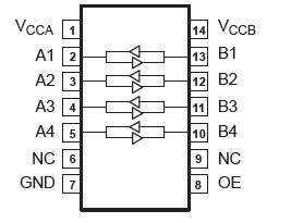 Specifications
| |
Rating |
Unit |
| VCCA |
Supply voltage range |
-0.5 to 4.6 |
V |
| VCCB |
-0.5 to 6.5 |
V |
| VI |
Input voltage range(2) |
-0.5 to 6.5 |
V |
| VO |
Voltage range applied to any output in the high-impedance or power-off state(2) |
-0.5 to 6.5 |
V |
| VO |
Voltage range pplied to any output in the high or low state(2) (3) |
A port |
-0.5 to VCCA+ 0.5 |
V |
|
B port |
-0.5 to VCCB+ 0.5 |
V |
| IIK |
Input clamp current |
VI < 0 |
-50 |
mA |
| IOK |
Output clamp current |
VO < 0 |
-50 |
mA |
| IO |
Continuous output current |
|
±50 |
mA |
| Continuous current through VCCA, VCCB, or GND |
±100 |
mA |
| JA |
Package thermal impedance |
D package(4) |
86 |
°C/W |
|
GXU/ZXU package(4) |
TBD |
|
PW package(4) |
113 |
|
RGY package(5) |
47 |
| Tstg |
Storage temperature range |
-65 to 150 |
°C |
(1) Stresses beyond those listed under "absolute maximum ratings" may cause permanent damage to the device. These are stress ratings only, and functional operation of the device at these or any other conditions beyond those indicated under "recommended operating conditions" is not implied. Exposure to absolute-maximum-rated conditions for extended periods may affect device reliability.
(2) The input and output negative-voltage ratings may be exceeded if the input and output current ratings are observed.
(3) The value of VCCA and VCCB are provided in the recommended operating conditions table.
(4) The package thermal impedance is calculated in accordance with JESD 51-7.
(5) The package thermal impedance is calculated in accordance with JESD 51-5.
DescriptionThis TXB0104 4-bit noninverting translator uses two separate configurable power-supply rails. The A port is designed to track VCCA. VCCA accepts any supply voltage from 1.2 V to 3.6 V. The B port is designed to track VCCB. VCCB accepts any supply voltage from 1.65 V to 5.5 V. This allows for universal low-voltage bidirectional translation between any of the 1.2-V, 1.5-V, 1.8-V, 2.5-V, 3.3-V, and 5-V voltage nodes. VCCA should not exceed VCCB.
When the output-enable (OE) input is low, all outputs are placed in the high-impedance state. The TXB0104 is designed so that the OE input circuit is supplied by VCCA.
This TXB0104 is fully specified for partial-power-down applications using Ioff. The Ioff circuitry disables the outputs, preventing damaging current backflow through the device when it is powered down.
To ensure the high-impedance state of TXB0104 during power up or power down, OE should be tied to GND through a pulldown resistor; the minimum value of the resistor is determined by the current-sourcing capability of the driver.

 TXB0104 Data Sheet