Type
:
Supply Current
:
Maximum Operating Temperature
: + 85 C
Mounting Style
: SMD/SMT
Supply Voltage - Max
: 3.6 V, 5.5 V
Supply Voltage - Min
: 1.65 V, 2.3 V
Propagation Delay Time
: 260 ns
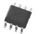
Package / Case
: WCSP-8
Features: ` Available in the Texas Instruments NanoStar™ and NanoFree™ Packages
` 1.65 V to 3.6 V on A port and 2.3 V to 5.5 V on B port (VCCA < VCCB)
` VCC Isolation Feature If Either VCC Input Is at GND, Both Ports Are in the High-Impedance State
` Ioff Supports Partial-Power-Down Mode Operation
` Latch-Up Performance Exceeds 100 mA Per JESD 78, Class II
` ESD Protection Exceeds JESD 22
A Port
2500-V Human-Body Model (A114-B)
250-V Machine Model (A115-A)
1500-V Charged-Device Model (C101)
B Port abc
8-kV Human-Body Model (A114-B)
250-V Machine Model (A115-A)
1500-V Charged-Device Model (C101)Pinout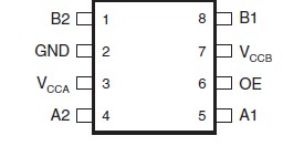 Specificationsover operating free-air temperature range (unless otherwise noted)
|
MIN MAX |
UNIT |
| VCCA |
Supply voltage range |
0.5 4.6 |
V |
| VCCB |
0.5 6.5 |
| VI Input voltage range |
A port |
0.5 4.6 |
V |
| B port |
0.5 6.5 |
|
Voltage range applied to any output
VO in the high-impedance or power-off state |
A port |
0.5 4.6 |
V |
| B port |
0.5 6.5 |
| VO Voltage range applied to any output in the high or low state |
A port |
0.5 VCCA + 0.5 |
V |
| B port |
0.5 VCCB + 0.5 |
| IIK Input clamp current |
VI < 0 |
50 |
mA |
| IOK Output clamp current |
VO < 0 |
50 |
mA |
| IO Continuous output current |
±50 |
mA |
| Continuous current through each VCCA, VCCB, or GND |
±100 |
mA |
| QJA Package thermal impedance(4) |
DCT package |
220 |
°C/W |
| DCU package |
227 |
| YZP package |
102 |
|
|
| Tstg Storage temperature range |
65 150 |
°C |
(1) Stresses beyond those listed under "absolute maximum ratings" may cause permanent damage to the device. These are stress ratings only, and functional operation of the device at these or any other conditions beyond those indicated under "recommended operating conditions" is not implied. Exposure to absolute-maximum-rated conditions for extended periods may affect device reliability.
(2) The input and output negative-voltage ratings may be exceeded if the input and output current ratings are observed.
(3) The value of VCCA and VCCB are provided in the recommended operating conditions table.
(4) The package thermal impedance is calculated in accordance with JESD 51-7.
DescriptionThis two-bit noninverting translator TXS0102YZPR uses two separate configurable power-supply rails. The A port is designed to track VCCA. VCCA accepts any supply voltage from 1.65 V to 3.6 V. The B port is designed to track VCCB. VCCA must be less than or equal to VCCB. VCCB accepts any supply voltage from 2.3 V to 5.5 V. This allows for low-voltage bidirectional translation between any of the 1.8-V, 2.5-V, 3.3-V, and 5-V voltage nodes.
When the output-enable (OE) input is low, all outputs are placed in the high-impedance state.
To ensure the high-impedance state during power up or power down, OE should be tied to GND through a pulldown resistor; the minimum value of the resistor is determined by the current-sourcing capability of the driver.
Parameters: | Technical/Catalog Information | TXS0102YZPR |
| Vendor | Texas Instruments (VA) |
| Category | Integrated Circuits (ICs) |
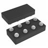
| Package / Case | 8-DSBGA |
| Packaging | Digi-Reel? |
| Input Type | Voltage |
| Output Type | Voltage |
| Supply Voltage | 1.65 V ~ 5.5 V |
| Data Rate | 24Mbs |
| Number of Channels | 2 |
| Operating Temperature | -40°C ~ 85°C |
| Drawing Number | 296; 4204741-4; YZP; 8 |
| Lead Free Status | Lead Free |
| RoHS Status | RoHS Compliant |
| Other Names | TXS0102YZPR
TXS0102YZPR
296 21932 6 ND
296219326ND
296-21932-6
|

 TXS0102YZPR Data Sheet