UT8Q512K32

Features: *25ns maximum (3.3 volt supply) address access time* MCM contains four (4) 512K x 8 industry-standard asynchronous SRAMs; the control architecture allows operation as 8, 16, 24, or 32-bit data width* TTL compatible inputs and output levels, three-state bidirectional data bus* Typical rad...

product image

UT8Q512K32 Picture
SeekIC No. : 004539123 Detail

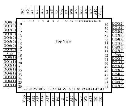
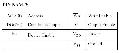
UT8Q512K32: Features: *25ns maximum (3.3 volt supply) address access time* MCM contains four (4) 512K x 8 industry-standard asynchronous SRAMs; the control architecture allows operation as 8, 16, 24, or 32-bit ...

floor Price/Ceiling Price

Part Number:
UT8Q512K32
Supply Ability:
5000

Price Break

  • Qty
  • 1~5000
  • Unit Price
  • Negotiable
  • Processing time
  • 15 Days
Total Cost: $ 0.00

SeekIC Buyer Protection PLUS - newly updated for 2013!

  • Escrow Protection.
  • Guaranteed refunds.
  • Secure payments.
  • Learn more >>

Month Sales

268 Transactions

Rating

evaluate  (4.8 stars)

Upload time: 2024/4/22

Payment Methods

All payment methods are secure and covered by SeekIC Buyer Protection PLUS.

Notice: When you place an order, your payment is made to SeekIC and not to your seller. SeekIC only pays the seller after confirming you have received your order. We will also never share your payment details with your seller.
Product Details

Description


Features:

* 25ns maximum (3.3 volt supply) address access time
* MCM contains four (4) 512K x 8 industry-standard
   asynchronous SRAMs; the control architecture allows
   operation as 8, 16, 24, or 32-bit data width
* TTL compatible inputs and output levels, three-state
   bidirectional data bus
* Typical radiation performance
   - Total dose: 50krads
   - SEL Immune >80 MeV-cm2/mg
   - LETTH(0.25) = >10 MeV-cm2/mg
   - Saturated Cross Section cm2 per bit, 5.0E-9
   - <1E-8 errors/bit-day, Adams 90% geosynchronous
   heavy ion
* Packaging options:
   - 68-lead dual cavity ceramic quad flatpack (CQFP) -
   (weight 7.37 grams)
* Standard Microcircuit Drawing 5962-01533
   - QML T and Q compliant part


Pinout

  Connection Diagram
  Connection Diagram


Specifications

SYMBOL               PARAMETER LIMITS
VDD DC supply voltage -0.5 to 4.6V
VI/O Voltage on any pin -0.5 to 4.6V
TSTG Storage temperature -65 to +150
PD Maximum power dissipation 1.0W (per byte)
TJ Maximum junction temperature2 +150
QJC Thermal resistance, junction-to-case3 10°C/W
II DC input current ±10 mA


Description

Each die in the UT8Q512K32 has three control inputs called Enable (En), Write Enable (Wn), and Output Enable (G); 19 address inputs, A(18:0); and eight bidirectional data lines, DQ(7:0). The UT8Q512K32 enable (En) controls device selection, active, and standby modes. Asserting En enables the device, causes IDD to rise to its active value, and decodes the 19 address inputs to each memory die by selecting the 2,048,000 byte of memory. Wn controls read and write operations. During a read cycle, G must be asserted to enable the outputs.


Customers Who Bought This Item Also Bought

Margin,quality,low-cost products with low minimum orders. Secure your online payments with SeekIC Buyer Protection.
Test Equipment
RF and RFID
Audio Products
Cables, Wires
Integrated Circuits (ICs)
Soldering, Desoldering, Rework Products
View more