VEC2603

Features: • A composite type of a low on-resistance P-channel MOSFET and a small signal N-channel MOSFET for driving P-channel MOSFET enables high-density mounting.• Best suited for load switches.• 1.8V drive.• 0.75mm mount highPinoutSpecifications Absolute max...

product image

VEC2603 Picture
SeekIC No. : 004541083 Detail

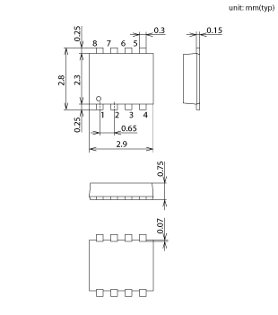
VEC2603: Features: • A composite type of a low on-resistance P-channel MOSFET and a small signal N-channel MOSFET for driving P-channel MOSFET enables high-density mounting.• Best suited for load...

floor Price/Ceiling Price

Part Number:
VEC2603
Supply Ability:
5000

Price Break

  • Qty
  • 1~5000
  • Unit Price
  • Negotiable
  • Processing time
  • 15 Days
Total Cost: $ 0.00

SeekIC Buyer Protection PLUS - newly updated for 2013!

  • Escrow Protection.
  • Guaranteed refunds.
  • Secure payments.
  • Learn more >>

Month Sales

268 Transactions

Rating

evaluate  (4.8 stars)

Upload time: 2024/4/28

Payment Methods

All payment methods are secure and covered by SeekIC Buyer Protection PLUS.

Notice: When you place an order, your payment is made to SeekIC and not to your seller. SeekIC only pays the seller after confirming you have received your order. We will also never share your payment details with your seller.
Product Details

Description


Features:

• A composite type of a low on-resistance P-channel MOSFET and a small signal N-channel MOSFET for driving P-channel MOSFET enables high-density mounting.
• Best suited for load switches.
• 1.8V drive.
• 0.75mm mount high


Pinout


Specifications

Absolute maximum ratings
(Pch) VDSS [V] 12
(Pch) VGSS [V] 8
(Pch) ID [A] 4
(Pch) PD [W] 0.9
When mounted on ceramic substrate (900mm²*0.8mm) 1unit
(Nch) VDSS [V] 30
(Nch) VGSS [V] 10
(Nch) ID [A] 0.15
(Nch) PD [W] 0.9
When mounted on ceramic substrate (900mm²*0.8mm) 1unit
Electrical characteristics
(Pch) VGS(off) min to max [V] 0.3 to 1.0
(Pch) |yfs| typ [S] 7.6
(Pch) RDS(on)1 typ [] 0.057
(Pch) RDS(on)1 max [] 0.08
(Pch) VGS [V] 2.5
(Pch) ID [A] 1
(Pch) RDS(on)2 typ [] 0.078
(Pch) RDS(on)2 max [] 0.112
(Pch) VGS [V] 1.8
(Pch) ID [A] 0.3
(Pch) Ciss [pF] 940
(Pch) Qg [nC] 11
(Nch) VGS(off) min to max [V] 0.4 to 1.3
(Nch) |yfs| typ [S] 0.22
(Nch) RDS(on)1 typ [] 3.7
(Nch) RDS(on)1 max [] 5.2
(Nch) VGS [V] 2.5
(Nch) ID [A] 0.04
(Nch) RDS(on)2 typ [] 6.4
(Nch) RDS(on)2 max [] 12.8
(Nch) VGS [V] 1.5
(Nch) ID [A] 0.01
(Nch) Ciss [pF] 7
(Nch) Qg [nC] 1.58


Parameter Symbol Conditions N-channel P-channel Unit
Drain-to-Source Voltage VDSS
30 -12 V
Gate-to-Source Voltage VGSS ±10 ±8 V
Drain Current (DC) ID 0.15 -4 A
Drain Current (Pulse) IDP PW10s, duty cycle1% 0.6 -16 A
Allowable Power Dissipation PD Mounted on a ceramic board (900mm2✕0.8mm)1unit 0.9 0.9 W
Channel Temperature Tch 150 150
Storage Temperature Tstg -55to+150 -55to+150


Customers Who Bought This Item Also Bought

Margin,quality,low-cost products with low minimum orders. Secure your online payments with SeekIC Buyer Protection.
RF and RFID
Static Control, ESD, Clean Room Products
Connectors, Interconnects
Prototyping Products
DE1
Line Protection, Backups
Circuit Protection
View more