VG3664321(4)1(2)BT

Features: • Single 3.3V (±0.3V ) power supply• High speed clock cycle time : 8/10 for LVTTL• High speed clock cycle time : 8/10 for SSTL - 3• Fully synchronous with all signals referenced to a positive clock edge• ProgrammableCAS Iatency (2,3)• Programmable burs...

product image

VG3664321(4)1(2)BT Picture
SeekIC No. : 004541351 Detail

VG3664321(4)1(2)BT: Features: • Single 3.3V (±0.3V ) power supply• High speed clock cycle time : 8/10 for LVTTL• High speed clock cycle time : 8/10 for SSTL - 3• Fully synchronous with all signa...

floor Price/Ceiling Price

Part Number:
VG3664321(4)1(2)BT
Supply Ability:
5000

Price Break

  • Qty
  • 1~5000
  • Unit Price
  • Negotiable
  • Processing time
  • 15 Days
Total Cost: $ 0.00

SeekIC Buyer Protection PLUS - newly updated for 2013!

  • Escrow Protection.
  • Guaranteed refunds.
  • Secure payments.
  • Learn more >>

Month Sales

268 Transactions

Rating

evaluate  (4.8 stars)

Upload time: 2024/4/24

Payment Methods

All payment methods are secure and covered by SeekIC Buyer Protection PLUS.

Notice: When you place an order, your payment is made to SeekIC and not to your seller. SeekIC only pays the seller after confirming you have received your order. We will also never share your payment details with your seller.
Product Details

Description


Features:

• Single 3.3V (±0.3V  ) power supply
• High speed clock cycle time : 8/10 for LVTTL
• High speed clock cycle time : 8/10 for SSTL - 3
• Fully synchronous with all signals referenced to a positive clock edge
• Programmable CAS Iatency (2,3)
• Programmable burst length (1,2,4,8,& Full page)
• Programmable wrap sequence (Sequential/Interleave)
• Automatic precharge and controlled precharge
• Auto refresh and self refresh modes
• Dual Internal banks controlled by A11 (Bank select) for VG36643211(2)
• Quad Internal banks controlled by A11 & A12 (Bank select) for VG36643241(2)
• Each Banks can operate simultaneously and independently
• LVTTL compatible I/O interface for VG36643211 and VG36643241
• SSTL - 3 compatible I/O interface for VG36643212 and VG36643242
• Random column access in every cycle
• x32 organization
• Input/Output controlled by DQM0 ~ 3
• 4,096 refresh cycles/64ms
• Burst termination by burst stop and precharge command
• Burst read/single write option


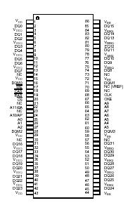
Pinout

  Connection Diagram


Specifications

Parameter Symbol Value Unit
Voltage on any pin relative to Vss
VIN,VOUT -0.5 to + 4.6 V
Supply voltage relative to Vss VDD,VDDQ -0.5 to + 4.6 V
Short circuit output current IOUT 50 mA
Power dissipation PD 1.0 W
Operating temperature TOPT 0 to + 70
Storage temperature TSTG -55 to + 125


Description

The VG3664321(4)1(2)BT is CMOS Synchronous Dynamic RAM organized as 524,288 - word x 32 - bit x 4 -bank, and 1,048,576 - word x 32 - bit x 2 - bank, respectively. VG3664321(4)1(2)BT is fabricated with an advanced submicron CMOS technology and designed to operate from a singly 3.3V only power supply. It is packaged in JEDEC standard pinout and standard plastic TSOP package.


Customers Who Bought This Item Also Bought

Margin,quality,low-cost products with low minimum orders. Secure your online payments with SeekIC Buyer Protection.
Connectors, Interconnects
LED Products
Fans, Thermal Management
Power Supplies - Board Mount
Isolators
View more