On Time (Max)
:
Off Time (Max)
:
Maximum Operating Temperature
:
Number of Outputs
: 1
Mounting Style
: Through Hole
Package / Case
: TO-220AB
On Resistance (Max)
: 35 mOhms
Operating Supply Voltage
: 18 V
Supply Current (Max)
: 0.1 mA
Features: During normal operation, the INPUT pin is electrically connected to the gate of the internal power MOSFET through a low impedance path.The device then behaves like a standard power MOSFET and can be used as a switch from DC up to 50KHz. The only difference from the user's standpoint is that a small DC current IISS (typ.100mA) flows into the INPUT pin in order to supply the internal circuitry.
The device integrates:
- OVERVOLTAGE CLAMP PROTECTION:internally set at 45V, along with the rugged avalanche characteristics of the Power MOSFET stage give this device unrivalled ruggedness and energy handling capability. This feature is mainly important when driving inductive loads.
- LINEAR CURRENT LIMITER CIRCUIT:limits the drain current ID to Ilim whatever the INPUT pin voltages. When the current limiter is active, the device operates in the linear region, so power dissipation may exceed the capability of the heatsink. Both case and junction temperatures increase, and if this phase lasts long enough,junction temperature may reach the overtemperature threshold Tjsh.
- OVERTEMPERATURE AND SHORT CIRCUIT PROTECTION:these are based on sensing the chip temperature and are not dependent on the input voltage. The location of the sensing element on the chip in the power stage area ensures fast, accurate detection of the junction temperature. Overtemperature cutout occurs in the range 150 to 190 °C, a typical value being 170 °C. The device is automatically restarted when the chip temperature falls of about 15 C below shut-down temperature.
- STATUS FEEDBACK:in the case of an overtemperature fault condition (Tj > Tjsh), the device tries to sink a diagnostic current Igf through the INPUT pin in order to indicate fault condition. If driven from a low impedance source, this current may be used in order to warn the control circuit of a device shutdown. If the drive impedance is high enough so that the INPUT pin driver is not able to supply the current Igf, the INPUT pin will fall to 0V. This will not however affect the device operation:no requirement is put on the current capability of the INPUT pin driver except to be able to supply the normal operation drive current IISS.
Additional features of this device are ESD protection according to the Human Body model and the ability to be driven from a TTL Logic circuit.
Pinout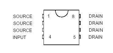 Specifications
| Symbol |
Parameter |
Value |
Unit |
| SO-8 |
DPAK |
TO-220 |
IPAK |
D2PAK |
| VDS |
Drain-source Voltage (VIN = 0) |
Internally Clamped |
V |
|
VIN |
Input Voltage |
Internally Clamped |
V |
| IIN |
Input Current |
+/-20 |
mA |
|
RIN MIN |
Minimum Input Series Impedance |
10 |
|
|
ID |
Drain Current |
Internally Clamped |
A |
| IR |
Reverse DC Output Current |
-15 |
A |
| VESD1 |
Electrostatic discharge(R=1.5 K,C= 100 pF) |
4000 |
V |
|
VESD2 |
Electrostatic Discharge on output pin only
R=330, C=150pF) |
16500 |
V |
|
Ptot |
Total Dissipation at TC=25°C |
4.6 |
74 |
74 |
74 |
74 |
W |
|
EMAX |
Maximum Switching Energy (L=0.4mH;
RL=0; Vbat=13.5V; Tjstart=150ºC; IL=18A) |
|
93 |
|
|
93 |
mJ |
| Tj |
Operating Junction Temperature |
Internally Limited |
|
| TC |
Case operating temperature |
Internally Limited |
|
|
Tstg |
Storage Temperature |
-55 to 150 |
|
DescriptionThe VNB14NV04, VND14NV04, VND14NV04-1,VNP14NV04, VNS14NV04, are monolithic devices designed in STMicroelectronics VIPower M0-3 Technology, intended for replacement of standard Power MOSFETS from DC up to 50KHz applications. Built in thermal shutdown, linear current limitation |and overvoltage clamp protect the chip in harsh environments.
Fault feedback of VNB14NV04, VND14NV04, VND14NV04-1,VNP14NV04, VNS14NV04 can be detected by monitoring the voltage at the input pin.
Parameters: | Technical/Catalog Information | VNP14NV04 |
| Vendor | STMicroelectronics |
| Category | Integrated Circuits (ICs) |
| Package / Case | TO-220-3 (Straight Leads) |
| Mounting Type | Through Hole |
| Type | Low Side |
| Voltage - Supply | - |
| On-State Resistance | 35 mOhm |
| Current - Output / Channel | - |
| Current - Peak Output | 18A |
| Packaging | Tube |
| Input Type | Non-Inverting |
| Number of Outputs | 1 |
| Operating Temperature | - |
| Drawing Number | * |
| Lead Free Status | Lead Free |
| RoHS Status | RoHS Compliant |
| Other Names | VNP14NV04
VNP14NV04
|

 VNP14NV04 Data Sheet


