VSC7124

Features: • ANSI X3T11 Fibre Channel Compliant at 1.0625Gb/s• IEEE 802.3z Gigabit Ethernet Compliant at 1.25Gb/s• Five Port Bypass Circuits (PBCs)• On-Chip Transmit Termination• 3.3V, 0.25W Typical Power• 0.35um CMOS, a Velocity Family Member• 44-Pin, 10mm...

product image

VSC7124 Picture
SeekIC No. : 004543338 Detail

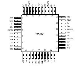
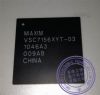
VSC7124: Features: • ANSI X3T11 Fibre Channel Compliant at 1.0625Gb/s• IEEE 802.3z Gigabit Ethernet Compliant at 1.25Gb/s• Five Port Bypass Circuits (PBCs)• On-Chip Transmit Terminati...

floor Price/Ceiling Price

Part Number:
VSC7124
Supply Ability:
5000

Price Break

  • Qty
  • 1~5000
  • Unit Price
  • Negotiable
  • Processing time
  • 15 Days
Total Cost: $ 0.00

SeekIC Buyer Protection PLUS - newly updated for 2013!

  • Escrow Protection.
  • Guaranteed refunds.
  • Secure payments.
  • Learn more >>

Month Sales

268 Transactions

Rating

evaluate  (4.8 stars)

Upload time: 2024/4/27

Payment Methods

All payment methods are secure and covered by SeekIC Buyer Protection PLUS.

Notice: When you place an order, your payment is made to SeekIC and not to your seller. SeekIC only pays the seller after confirming you have received your order. We will also never share your payment details with your seller.
Product Details

Description


Features:

• ANSI X3T11 Fibre Channel Compliant at 1.0625Gb/s
• IEEE 802.3z Gigabit Ethernet Compliant at 1.25Gb/s
• Five Port Bypass Circuits (PBCs)
• On-Chip Transmit Termination
• 3.3V, 0.25W Typical Power
• 0.35um CMOS, a Velocity Family Member
• 44-Pin, 10mm PQFP Package


Pinout

  Connection Diagram


Specifications

TTL Power Supply Voltage (VDD)............................................................................................... 0.5V to +4V
PECL DC Input Voltage (VINP) ...................................................................................... -0.5V to VDD +0.5V
TTL DC Input Voltage, (VINT).................................................................................................. -0.5V to 5.5V
DC Voltage Applied to Outputs for High Output State (VIN TTL) ................................. -0.5V to VDD + 0.5V
TTL Output Current (IOUT), (DC, Output High).................................................................................. 50mA
PECL Output Current (IOUT), (DC, Output High) ..............................................................................-50mA
Case Temperature Under Bias, (TC).............................................................................. -55°C to +125°C
Storage Temperature (TSTG)....................................................................................... -65°C to + 150°C


Description

The VSC7124 contains five cascaded Port Bypass Circuits (PBCs) used to steer serial signals. This part is typically sed in distributing Fibre Channel signals to an array of disk drives in an FC-AL loop as illustrated in Figure . The VSC7124 can be used with any of the Vitesse JBOD circuits to implement FC-AL JBODs of irtually any size. In Figure 1, the first VSC7127's CRU is configured as a Repeater to attenuate jitter. The SC7124 does not contain a CRU in order to reduce power and cost. The second VSC7127's CRU is configureds a retimer so that the output of the device is a jitter compliance point.

Each PBC is a multiplexer that is controlled by the corresponding SELx line which, if HIGH, selects the external nput or, if LOW, selects the output of the previous PBC.


Customers Who Bought This Item Also Bought

Margin,quality,low-cost products with low minimum orders. Secure your online payments with SeekIC Buyer Protection.
Connectors, Interconnects
Potentiometers, Variable Resistors
Resistors
Discrete Semiconductor Products
Audio Products
View more