Features: • Maximized EMI suppression using Cypress's Spread Spectrum technology
• I2C interface
• Four copies of CPU Output
• Six copies of PCI Output
• Two copies of AGP Output
• One copy of 48-MHz USB Output
• One copy of 24-MHz SIO Output
• Twelve copies of SDRAM Output
• One buffered copy of 14.318-MHz reference input
• Mode input pin selects optional power management input control pins (reconfigures pins 29, 30, 31, and 32)
• Smooth frequency transition upon frequency reselection
• Available in 48-pin SSOP (300 mils)
• Standard W127 device supports up to 112-MHz operations. High-performance option W127-A supports up to 124-MHz.Pinout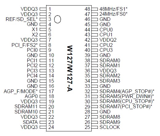 Specifications
Stresses greater than those listed in this table may cause permanent damage to the device. These represent a stress rating only. Operation of the device at these or any other conditions above those specified in the operating sections of this specification is not implied. Maximum conditions for extended periods may affect reliability.
|
Parameter |
Description |
Rating |
Unit |
|
VDDQ3, VIN |
Voltage on any Pin with Respect to GND |
0.5 to +7.0 |
V |
|
TSTG |
Storage Temperature |
65 to +150 |
|
|
TB |
Ambient Temperature under Bias |
55 to +125 |
|
|
TA |
Operating Temperature |
0 to +70 |
|
|
ESDPROT |
Input ESD Protection |
2 (min.) |
kV |
DescriptionPins 3, 8, 17, 47, and 48 are dual-purpose l/O pins. Upon power-up these pins act as logic inputs, allowing the determination of assigned device functions. A short time after powerup, the logic state of each pin is latched and the pins then become clock outputs. This feature reduces device pin count by combining clock outputs with input select pins.
An external 10-k "strapping" resistor is connected between each l/O pin and ground or VDDQ3. Connection to ground sets a latch to "0," connection to VDDQ3 sets a latch to "1." Figure 1 and Figure 2 show two suggested methods for strapping resistor connection.
Upon W127/W127-A power-up, the first 2 ms of operation is used for input logic selection. During this period, the 24-MHz, 48-MHz, REF, PCI_F and AGP_F clock output buffers are three-stated, allowing the output strapping resistor on each l/O pin to pull the pin and its associated capacitive clock load to either a logic HIGH or logic LOW state. At the end of the 2-ms period, the established logic 0 or 1 condition of each l/O pin is latched. Next the output buffers are enabled, converting all l/O pins into operating clock outputs. The 2-ms timer starts when VDDQ3 reaches 2.0V. The input bits can only be reset by turning VDDQ3 off and then back on again.
W127-A should be noted that the strapping resistors have no significant effect on clock output signal integrity. The drive impedance of the clock output is 40 (nominal), which is minimally affected by the 10-k strap to ground or VDDQ3. As with the series termination resistor, the output strapping resistor should be placed as close to the l/O pin as possible in order to keep the interconnecting trace short. The trace from the resistor to ground or VDDQ3 should be kept less than two inches in length to prevent system noise coupling during input logic sampling.
When the clock outputs are enabled following the 2-ms input period, target (normal) output frequency is delivered, assuming that VDDQ3 has stabilized. If VDDQ3 has not yet reached full value, output frequency initially may be below target but will increase to target once VDDQ3 voltage has stabilized. In either case, a short output clock cycle may be produced from the CPU clock outputs when the outputs are enabled.

 W127-A Data Sheet


