W19B160BT

Features: Performance• 2.7~3.6-volt write (program and erase) operations• Fast write operation− Sector erase time: 0.7s (Typical)− Chip erases time: 25 s (Typical)− Byte/Word programming time: 5/7 µs (Typical)• Read access time: 70 ns• Typical progra...

product image

W19B160BT Picture
SeekIC No. : 004544450 Detail

W19B160BT: Features: Performance• 2.7~3.6-volt write (program and erase) operations• Fast write operation− Sector erase time: 0.7s (Typical)− Chip erases time: 25 s (Typical)− Byt...

floor Price/Ceiling Price

Part Number:
W19B160BT
Supply Ability:
5000

Price Break

  • Qty
  • 1~5000
  • Unit Price
  • Negotiable
  • Processing time
  • 15 Days
Total Cost: $ 0.00

SeekIC Buyer Protection PLUS - newly updated for 2013!

  • Escrow Protection.
  • Guaranteed refunds.
  • Secure payments.
  • Learn more >>

Month Sales

268 Transactions

Rating

evaluate  (4.8 stars)

Upload time: 2024/4/26

Payment Methods

All payment methods are secure and covered by SeekIC Buyer Protection PLUS.

Notice: When you place an order, your payment is made to SeekIC and not to your seller. SeekIC only pays the seller after confirming you have received your order. We will also never share your payment details with your seller.
Product Details

Description


Features:

Performance
• 2.7~3.6-volt write (program and erase) operations
• Fast write operation
− Sector erase time: 0.7s (Typical)
− Chip erases time: 25 s (Typical)
− Byte/Word programming time: 5/7 µs (Typical)
• Read access time: 70 ns
• Typical program/erase cycles:
− 100K
• Twenty-year data retention
• Ultra low power consumption
− Active current (Read): 9mA (Typical)
− Active current (Program/erase): 20mA (Typical)
− Standby current: 0.2 A (Typical)
Architecture
• Sector erases architecture
− One 16Kbyte, two 8Kbyte, one 32Kbyte, and thirty-one 64Kbyte sectors
− Top or bottom boot block configurations available
− Supports full chip erase
• JEDEC standard byte-wide and word-wide pin-outs TTL compatible I/O
• Manufactured on WinStack-S 0.13µm process technology
• Available packages: 48-pin TSOP and 48-ball TFBGA (6x8mm)
Software Features
• Compatible with common Flash Memory Interface (CFI) specification
− Flash device parameters stored directly on the device
− Allows software driver to identify and use a variety of different current and future Flash products
• End of program detection
− Software method: Toggle bit/Data polling
• Erase Suspend /Erase Resume
− Suspend an erase operation to read data or program data.
− Resume erase suspend operation.
• Unlock bypass program command
− Allows the system to program bytes or words to device faster than standard program command.
Hardware Features
• Ready/#Busy output (RY/#BY)
− Detect program or erase cycle completion
• Hardware reset pin (#RESET)
− Reset the internal state machine to the read mode
• Sector Protection
− Sectors can be locked in-system or via programmer
− Temporary Sector Unprotect allows changing data in protected sectors in-system
Temperature range
• Extended temperature range (-20 to 85 )
• Industrial devices ambient temperature(-40 to +85 )


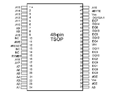
Pinout

  Connection Diagram


Specifications

PARAMETER
RATING
UNIT
Storage Temperature Plastic Packages
Ambient Temperature with Power Applied
Voltage with Respect to Ground , VDD (Note1)
A9, #OE, and #RESET (Note 2)
All other pins (Note 1)
Output Short Circuit Current (Note 3)
-65 to +150
-65 to +125
-0.5 to +4.0
-0.5 to VDD (Max.)
-0.5 to VDD +0.5
200
°C
°C
V
V
V
mA
Notes:
1. Minimum DC voltage on input or I/O pins is 0.5 V. During voltage transitions, input or I/O pins may overshoot VSS to -
2.0 V for periods of up to 20 ns. Maximum DC voltage on input or I/O pins is VDD +0.5 V. During voltage transitions, input or I/O pins may overshoot to VDD +2.0 V for periods up to 20 ns.
2. Minimum DC input voltage on pins A9, #OE, and #RESET is -0.5 V. During voltage transitions, A9, #OE, and #RESET may overshoot VSS to -2.0 V for periods of up to 20 ns. Maximum DC input voltage on pin A9 is VDD (Max.) which may overshoot to +14.0 V for periods up to 20 ns. Maximum DC input voltage is +9.5 V which may overshoot to +12.0 V for periods up to 20 nS.
3. No more than one output may be shorted to ground at a time. Duration of the short circuit should not be greater than one second.


Description

The W19B160B is a 16Mbit, 2.7~3.6 volt CMOS flash memory organized as 2M × 8 or 1M × 16 bits. For flexible erase capability, the 16Mbits of data are divided into one 16Kbyte, two 8Kbyte, one 32Kbyte, and thirty-one 64Kbyte sectors. The word-wide (× 16) data appears on DQ15-DQ0, and byte-wide (× 8) data appears on DQ7−DQ0. The device can be programmed and erased in-system with a standard 2.7~3.6V power supply. A 12-volt VPP is not required. The unique cell architecture of the W19B160B results in fast program/erase operations with extremely low current consumption. The device can also be programmed and erased by using standard EPROM programmers.


Customers Who Bought This Item Also Bought

Margin,quality,low-cost products with low minimum orders. Secure your online payments with SeekIC Buyer Protection.
Integrated Circuits (ICs)
Power Supplies - External/Internal (Off-Board)
Crystals and Oscillators
Boxes, Enclosures, Racks
View more