WM2125

Features: • Two 10-bit resolution ADCs• 40MSPS conversion rate• Programmable clock / output data formats − 10-bit multiplexed or 20-bit wide output − Input clock at sample rate or twice sample rate for multiplexed output − Output clocks for output data sampling&...

product image

WM2125 Picture
SeekIC No. : 004546064 Detail

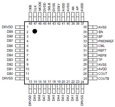
WM2125: Features: • Two 10-bit resolution ADCs• 40MSPS conversion rate• Programmable clock / output data formats − 10-bit multiplexed or 20-bit wide output − Input clock at sam...

floor Price/Ceiling Price

Part Number:
WM2125
Supply Ability:
5000

Price Break

  • Qty
  • 1~5000
  • Unit Price
  • Negotiable
  • Processing time
  • 15 Days
Total Cost: $ 0.00

SeekIC Buyer Protection PLUS - newly updated for 2013!

  • Escrow Protection.
  • Guaranteed refunds.
  • Secure payments.
  • Learn more >>

Month Sales

268 Transactions

Rating

evaluate  (4.8 stars)

Upload time: 2024/4/15

Payment Methods

All payment methods are secure and covered by SeekIC Buyer Protection PLUS.

Notice: When you place an order, your payment is made to SeekIC and not to your seller. SeekIC only pays the seller after confirming you have received your order. We will also never share your payment details with your seller.
Product Details

Description


Features:

• Two 10-bit resolution ADCs
• 40MSPS conversion rate
• Programmable clock / output data formats
  − 10-bit multiplexed or 20-bit wide output
  − Input clock at sample rate or twice sample rate for multiplexed output
  − Output clocks for output data sampling
• Precision internal voltage references
• Hardware mode selection
• Wide input bandwidth 300MHz
• Low power 240mW typical at 3.3V supplies
• Powerdown mode to less than 1mW
• 48-pin TQFP package


Application

The WM2125 is a dual channel 10-bit 40MSPS ADC which consumes only 240mW from a single 3.3V supply. The device is optimised for communications applications that require close matching between channels and a wide input bandwidth.

Input signals are differential for improved noise performance. Both A and B input channels are sampled simultaneously and are processed through matched signal paths and 10-bit multistage pipeline ADC. A number of different input clock / output data formats are supported including 20-bits wide at the sampling rate or 10-bits wide at twice the sampling rate, with additional clock outputs supplied by the device to latch the output data.

System design and power requirements are further simplified by the provision of an on-chip precision voltage reference. Alternatively, external references can be used if higher precision references are required.


Pinout

  Connection Diagram


Specifications

CONDITION
MIN
MAX
Digital supply voltage, DVDD to DVSS
-0.5V
+3.6V
Digital output driver supply voltage, DRVDD to DRVSS
-0.5V
+3.6V
Analogue supply voltage, AVDD to AVSS
-0.5V
+3.6V
Maximum ground difference between AVSS, DVSS and DRVSS
-0.5V
+0.5V
Voltage range digital inputs
DVSS 0.5V
DVDD + 0.5V
Voltage range analogue inputs (includes CLK pin)
AVSS - 0.5V
AVDD + 0.5V
Operating temperature range, TA
-45°C
+85°C
Storage temperature
-65°C
+150°C
Lead temperature (1.6mm from case for 10 seconds)
 
+300°C


Description

• I/Q demodulation for the WM2125
  − Wireless Local Loop (WLL)
  − Set Top Box (STB)
  − Cable Modem
• IF and Baseband Digitisation
• Test Instrumentation
• Medical Imaging


Customers Who Bought This Item Also Bought

Margin,quality,low-cost products with low minimum orders. Secure your online payments with SeekIC Buyer Protection.
Motors, Solenoids, Driver Boards/Modules
Static Control, ESD, Clean Room Products
Isolators
View more