X9260

Features: • DualTwo Separate Potentiometers• 256 resistor taps/pot0.4% resolution• SPI Serial Interface for write, read, and transfer operations of the potentiometer• Wiper Resistance, 100Ω typical @ V+ = 5V, V- = -5V• 4 Nonvolatile Data Registers for Each Poten...

product image

X9260 Picture
SeekIC No. : 004547490 Detail

X9260: Features: • DualTwo Separate Potentiometers• 256 resistor taps/pot0.4% resolution• SPI Serial Interface for write, read, and transfer operations of the potentiometer• Wiper R...

floor Price/Ceiling Price

Part Number:
X9260
Supply Ability:
5000

Price Break

  • Qty
  • 1~5000
  • Unit Price
  • Negotiable
  • Processing time
  • 15 Days
Total Cost: $ 0.00

SeekIC Buyer Protection PLUS - newly updated for 2013!

  • Escrow Protection.
  • Guaranteed refunds.
  • Secure payments.
  • Learn more >>

Month Sales

268 Transactions

Rating

evaluate  (4.8 stars)

Upload time: 2024/4/27

Payment Methods

All payment methods are secure and covered by SeekIC Buyer Protection PLUS.

Notice: When you place an order, your payment is made to SeekIC and not to your seller. SeekIC only pays the seller after confirming you have received your order. We will also never share your payment details with your seller.
Product Details

Description


Features:

• DualTwo Separate Potentiometers
• 256 resistor taps/pot0.4% resolution
• SPI Serial Interface for write, read, and transfer operations of the potentiometer
• Wiper Resistance, 100Ω typical @ V+ = 5V, V- = -5V
• 4 Nonvolatile Data Registers for Each Potentiometer
• Nonvolatile Storage of Multiple Wiper Positions
• Power-on Recall. Loads Saved Wiper Position on Power-up.
• Standby Current < 5µA Max
• VCC: 2.7V to 5.5V Operation
• 50kΩ, 100kΩ versions of End to End Resistance
• 100 yr. Data Retention
• Endurance: 100,000 Data Changes per Bit per Register
• 24-Lead SOIC, 24-Lead XBGA
• Low Power CMOS
• Power Supply VCC = 2.7V to 5.5V
V+ = 2.7V to 5.5V
V- = -2.7V to -5.5V


Application

• Vary the gain of a voltage amplifier
• Provide programmable dc reference voltages for comparators and detectors
• Control the volume in audio circuits
• Trim out the offset voltage error in a voltage amplifier circuit
• Set the output voltage of a voltage regulator
• Trim the resistance in Wheatstone bridge circuits
• Control the gain, characteristic frequency and Q-factor in filter circuits
• Set the scale factor and zero point in sensor signal conditioning circuits
• Vary the frequency and duty cycle of timer ICs
• Vary the dc biasing of a pin diode attenuator in RF circuits
• Provide a control variable (I, V, or R) in feedback circuits
• Adjust the contrast in LCD displays
• Control the power level of LED transmitters in communication systems
• Set and regulate the DC biasing point in an RF power amplifier in wireless systems
• Control the gain in audio and home entertainment systems
• Provide the variable DC bias for tuners in RF wireless systems
• Set the operating points in temperature control systems
• Control the operating point for sensors in industrial systems
• Trim offset and gain errors in artificial intelligent systems


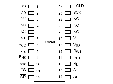
Pinout

  Connection Diagram


Specifications

Temperature under bias ........................-65 to +135
Storage temperature ............................ -65 to +150
Voltage on SCK, SCL or any address input
with respect to VSS .................................... -1V to +7V
Voltage on V+ (referenced to VSS)..........................10V
Voltage on V- (referenced to VSS)..........................-10V
(V+) - (V-) ...............................................................12V
Any VH/RH ................................................................V+
Any VL/RL............................................................VLead
temperature (soldering, 10 seconds).................. 300
IW (10 seconds)..................................................±6mA

Stresses above those listed under "Absolute Maximum Ratings" may cause permanent damage to the device. This is a stress rating only; the functional operation of the device (at these or any other conditions above those listed in the operational sections of this specification) is not implied. Exposure to absolute maximum rating conditions for extended periods may affect device reliability.


Description

The X9260 integrates 2 digitally controlled potentiometer (XDCP) on a monolithic CMOS integrated circuit. The X9260 digitally controlled potentiometer is implemented using 255 resistive elements in a series array. Between each element are tap points connected to the wiper terminal through switches. The position of the wiper on the array is controlled by the user through the SPI bus interface. Each X9260 potentiometer has associated with it a volatile Wiper Counter Register (WCR) and a four nononvolatile Data Registers that can be directly written to and read by the user. The contents of the WCR controls the position of the wiper on the resistor array though the switches. Power-up recalls the contents of the default Data Register (DR0) to the WCR. The XDCP can be used as a three-terminal potentiometer or as a two terminal variable resistor in a wide variety of applications including control, parameter adjustments, and signal processing.


Customers Who Bought This Item Also Bought

Margin,quality,low-cost products with low minimum orders. Secure your online payments with SeekIC Buyer Protection.
Boxes, Enclosures, Racks
Potentiometers, Variable Resistors
Discrete Semiconductor Products
Memory Cards, Modules
Cables, Wires - Management
Integrated Circuits (ICs)
View more