XC167CS-32F

Features: • Master or Slave mode operation• Full-duplex or Half-duplex transfers• Baudrate generation from 20 Mbit/s to 305.18 bit/s (@ 40 MHz)• Flexible data format Programmable number of data bits: 2 to 16 bits Programmable shift direction: LSB-first or MSB-first Progr...

product image

XC167CS-32F Picture
SeekIC No. : 004547699 Detail

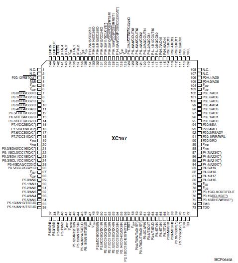
XC167CS-32F: Features: • Master or Slave mode operation• Full-duplex or Half-duplex transfers• Baudrate generation from 20 Mbit/s to 305.18 bit/s (@ 40 MHz)• Flexible data format Program...

floor Price/Ceiling Price

Part Number:
XC167CS-32F
Supply Ability:
5000

Price Break

  • Qty
  • 1~5000
  • Unit Price
  • Negotiable
  • Processing time
  • 15 Days
Total Cost: $ 0.00

SeekIC Buyer Protection PLUS - newly updated for 2013!

  • Escrow Protection.
  • Guaranteed refunds.
  • Secure payments.
  • Learn more >>

Month Sales

268 Transactions

Rating

evaluate  (4.8 stars)

Upload time: 2024/4/18

Payment Methods

All payment methods are secure and covered by SeekIC Buyer Protection PLUS.

Notice: When you place an order, your payment is made to SeekIC and not to your seller. SeekIC only pays the seller after confirming you have received your order. We will also never share your payment details with your seller.
Product Details

Description


Features:

• Master or Slave mode operation
• Full-duplex or Half-duplex transfers
• Baudrate generation from 20 Mbit/s to 305.18 bit/s (@ 40 MHz)
• Flexible data format
   Programmable number of data bits: 2 to 16 bits
   Programmable shift direction: LSB-first or MSB-first
   Programmable clock polarity: idle low or idle high
   Programmable clock/data phase: data shift with leading or trailing clock edge
• Loop back option available for testing purposes
• Interrupt generation on transmitter buffer empty condition, receive buffer full condition, error condition (receive, phase, baudrate, transmit error)
• Three pin interface with flexible SSC pin configuration


Pinout

  Connection Diagram


Specifications

Parameter
Symbol
Limit Values
Unit
Notes
Min.
Max.
Storage temperature
TST
-65
150
°C
-
Junction temperature
TJ
-40
150
°C
under bias
Voltage on VDDI pins with
respect to ground (VSS)
VDDI
-0.5
3.25
V
-
Voltage on VDDP pins with
respect to ground (VSS)
VDDP
-0.5
6.2
V
-
Voltage on any pin with
respect to ground (VSS)
VIN
-0.5
VDDP +0.5
V
-
Input current on any pin
during overload condition
-
-10
10
mA
-
Absolute sum of all input
currents during overload
condition
-
-
|100|
mA
-


Description

The architecture of the XC167 combines advantages of RISC, CISC, and DSP processors with an advanced peripheral subsystem in a very well-balanced way. In addition, the on-chip memory blocks allow the design of compact systems-on-silicon with maximum performance (computing, control, communication).

The XC167 on-chip memory blocks (program code-memory and SRAM, dual-port RAM, data SRAM) and the set of generic peripherals are connected to the CPU via separate buses. Another bus, the LXBus, connects additional on-chip resources as well as external resources (see Figure 3). This bus structure enhances the overall system performance by enabling the concurrent operation of several subsystems of the XC167.

The following block diagram of XC167 gives an overview of the different on-chip components and of the advanced, high bandwidth internal bus structure of the XC167.


Customers Who Bought This Item Also Bought

Margin,quality,low-cost products with low minimum orders. Secure your online payments with SeekIC Buyer Protection.
Transformers
Resistors
Power Supplies - External/Internal (Off-Board)
Computers, Office - Components, Accessories
View more