XC5VLX330-1FF1760I4068

PinoutDescriptionThe XC5VLX330-1FF1760I4068 is designed as one kind of platform flash in-system programmable configuration PROM device that generates a configuration clock that drives the PROM. And this device includes 32-Mbit, 16-Mbit, and 8-Mbit PROMs that support Master Serial, Slave Serial, Ma...

product image

XC5VLX330-1FF1760I4068 Picture
SeekIC No. : 004547899 Detail

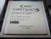
XC5VLX330-1FF1760I4068: PinoutDescriptionThe XC5VLX330-1FF1760I4068 is designed as one kind of platform flash in-system programmable configuration PROM device that generates a configuration clock that drives the PROM. And ...

floor Price/Ceiling Price

Part Number:
XC5VLX330-1FF1760I4068
Supply Ability:
5000

Price Break

  • Qty
  • 1~5000
  • Unit Price
  • Negotiable
  • Processing time
  • 15 Days
Total Cost: $ 0.00

SeekIC Buyer Protection PLUS - newly updated for 2013!

  • Escrow Protection.
  • Guaranteed refunds.
  • Secure payments.
  • Learn more >>

Month Sales

268 Transactions

Rating

evaluate  (4.8 stars)

Upload time: 2024/4/24

Payment Methods

All payment methods are secure and covered by SeekIC Buyer Protection PLUS.

Notice: When you place an order, your payment is made to SeekIC and not to your seller. SeekIC only pays the seller after confirming you have received your order. We will also never share your payment details with your seller.
Product Details

Description


Pinout

  Connection Diagram


Description

The XC5VLX330-1FF1760I4068 is designed as one kind of platform flash in-system programmable configuration PROM device that generates a configuration clock that drives the PROM. And this device includes 32-Mbit, 16-Mbit, and 8-Mbit PROMs that support Master Serial, Slave Serial, Master SelectMAP, and Slave SelectMAP FPGA configuration modes.

Features of the XC5VLX330-1FF1760I4068 are:(1)In-System Programmable PROMs for Configuration of Xilinx FPGAs; (2)Low-Power Advanced CMOS NOR FLASH Process; (3)Endurance of 20,000 Program/Erase Cycles; (4)Operation over Full Industrial Temperature Range (-40 to +85); (5)IEEE Standard 1149.1/1532 Boundary-Scan (JTAG) Support for Programming, Prototyping, and Testing; (6)JTAG Command Initiation of Standard FPGA Configuration; (7)Cascadable for Storing Longer or Multiple Bitstreams; (8)Dedicated Boundary-Scan (JTAG) I/O Power Supply (VCCJ); (9)I/O Pins Compatible with Voltage Levels Ranging From 1.5V to 3.3V; (10)Design Support Using the Xilinx Alliance ISE and Foundation ISE Series Software Packages; (11)Built-in data decompressor compatible with Xilinx advanced compression technology; (12)Available in small-footprint VO48, VOG48, FS48, and FSG48 packages.

The absolute maximum ratings of the XC5VLX330-1FF1760I4068 can be summarized as:(1)Internal supply voltage relative to GND:0.5 to +2.7 V;(2)I/O supply voltage relative to GND:0.5 to +4.0 V;(3)JTAG I/O supply voltage relative to GND:0.5 to +4.0 V;(4)Input voltage with respect to GND:0.5 to +3.6 V;(5)Voltage applied to High-Z output:0.5 to +3.6 V;(6)Storage temperature (ambient):65 to +150 °C;(7)Junction temperature: +125 °C. If you want to know more information such as the electrical characteristics about the XC5VLX330-1FF1760I4068, please download the datasheet in www.seekic.com or www.chinaicmart.com.


Customers Who Bought This Item Also Bought

Margin,quality,low-cost products with low minimum orders. Secure your online payments with SeekIC Buyer Protection.
Tapes, Adhesives
803
Programmers, Development Systems
Integrated Circuits (ICs)
Boxes, Enclosures, Racks
Cable Assemblies
View more