XC9500XV

Features: • Optimized for high-performance 2.5V systems- 3.5 ns pin-to-pin logic delays- Small footprint packages including VQFPs, TQFPs and CSPs (Chip Scale Package)- Lower power operation- Multi-voltage operation- FastFLASH technology• Advanced system features- In-system programmable...

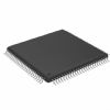
product image

XC9500XV Picture
SeekIC No. : 004548065 Detail

XC9500XV: Features: • Optimized for high-performance 2.5V systems- 3.5 ns pin-to-pin logic delays- Small footprint packages including VQFPs, TQFPs and CSPs (Chip Scale Package)- Lower power operation- M...

floor Price/Ceiling Price

Part Number:
XC9500XV
Supply Ability:
5000

Price Break

  • Qty
  • 1~5000
  • Unit Price
  • Negotiable
  • Processing time
  • 15 Days
Total Cost: $ 0.00

SeekIC Buyer Protection PLUS - newly updated for 2013!

  • Escrow Protection.
  • Guaranteed refunds.
  • Secure payments.
  • Learn more >>

Month Sales

268 Transactions

Rating

evaluate  (4.8 stars)

Upload time: 2024/3/28

Payment Methods

All payment methods are secure and covered by SeekIC Buyer Protection PLUS.

Notice: When you place an order, your payment is made to SeekIC and not to your seller. SeekIC only pays the seller after confirming you have received your order. We will also never share your payment details with your seller.
Product Details

Description


Features:

• Optimized for high-performance 2.5V systems
- 3.5 ns pin-to-pin logic delays
- Small footprint packages including VQFPs, TQFPs and CSPs (Chip Scale Package)
- Lower power operation
- Multi-voltage operation
- FastFLASH technology
• Advanced system features
- In-system programmable
- Output banking (XC95144XV, XC95288XV)
- Superior pin-locking and routability with FastCONNECT II™ switch matrix
- Extra wide 54-input Function Blocks
- Up to 90 product-terms per macrocell with individual product-term allocation
- Local clock inversion with three global and one product-term clocks
- Individual output enable per output pin with local inversion
- Input hysteresis on all user and boundary-scan pin inputs
- Bus-hold circuitry on all user pin inputs
- Full IEEE Standard 1149.1 boundary-scan (JTAG) support on all devices
• Four pin-compatible device densities
- 36 to 288 macrocells, with 800 to 6400 usable gates
• Fast concurrent programming
• Slew rate control on individual outputs
• Enhanced data security features
• Excellent quality and reliability
- 10,000 program/erase cycles endurance rating
- 20 year data retention
• Pin-compatible with 3.3V core XC9500XL family in common package footprints
• Hot Plugging capability


Description

Each XC9500XV device is a subsystem consisting of multiple Function Blocks (FBs) and I/O Blocks (IOBs) fully interconnected by the FastCONNECT II switch matrix. The IOB provides buffering for device inputs and outputs. Each FB provides programmable logic capability with extra wide 54 inputs and 18 outputs. The FastCONNECT II switch matrix connects all FB outputs and input signals to the FB inputs. For each FB, up to 18 outputs (depending on package pin-count) and associated output enable signals drive directly to the IOBs. See Figure 1.


Customers Who Bought This Item Also Bought

Margin,quality,low-cost products with low minimum orders. Secure your online payments with SeekIC Buyer Protection.
RF and RFID
Audio Products
Crystals and Oscillators
Prototyping Products
DE1
View more