Features: • 0.22 µm 5-layer epitaxial process
• QML certified
• Radiation hardened FPGAs for space and satellite applications
• Guaranteed total ionizing dose to 100K Rad(si)
• Latch-up immune to LET = 125 MeV cm2/mg
• SEU immunity achievable with recommended redundancy implementation
• Guaranteed over the full military temperature range (55 to +125)
• Fast, high-density Field-Programmable Gate Arrays
- Densities from 100k to 1M system gates
- System performance up to 200 MHz
- Hot-swappable for Compact PCI
• Multi-standard SelectI/O™ interfaces
- 16 high-performance interface standards
- Connects directly to ZBTRAM devices
• Built-in clock-management circuitry
- Four dedicated delay-locked loops (DLLs) for advanced clock control
- Four primary low-skew global clock distribution nets, plus 24 secondary global nets
• Hierarchical memory system
- LUTs configurable as 16-bit RAM, 32-bit RAM, 16-bit dual-ported RAM, or 16-bit Shift Register
- Configurable synchronous dual-ported 4k-bit RAMs
- Fast interfaces to external high-performance RAMs
• Flexible architecture that balances speed and density
- Dedicated carry logic for high-speed arithmetic
- Dedicated multiplier support
- Cascade chain for wide-input functions
- Abundant registers/latches with clock enable, and dual synchronous/asynchronous set and reset
- Internal 3-state bussing
- IEEE 1149.1 boundary-scan logic
- Die-temperature sensing device
• Supported by FPGA Foundation™ and Alliance Development Systems
- Complete support for Unified Libraries, Relationally Placed Macros, and Design Manager
- Wide selection of PC and workstation platforms
• SRAM-based in-system configuration
- Unlimited reprogrammability
- Four programming modes
• Available to Standard Microcircuit Drawings. Contact Defense Supply Center Columbus (DSCC) for more information at http://www.dscc.dla.mil
- 5962-99572 for XQVR300
- 5962-99573 for XQVR600
- 5962-99574 for XQVR1000
Specifications
| Symbol |
Description |
Min/Max |
Units |
| VCCINT |
Supply voltage relative to GND |
0.5 to 3.0 |
V |
| VCCO |
Supply voltage relative to GND |
0.5 to 4.0 |
V |
| VREF |
Input reference voltage |
0.5 to 3.6 |
V |
| VIN(3) |
Input voltage relative to GND |
Using VREF |
0.5 to 3.6 |
V |
| Internal threshold |
0.5 to 5.5 |
V |
| VTS |
Voltage applied to 3-state output |
0.5 to 5.5 |
V |
| VCC |
Longest supply voltage rise time from 1V to 2.375V |
50 |
ms |
| TSTG |
Storage temperature (ambient) |
65 to +150 |
|
| TJ |
Junction temperature |
+150 |
|
Notes:
1. Stresses beyond those listed under Absolute Maximum Ratings may cause permanent damage to the device. These are stress ratings only, and functional operation of the device at these or any other conditions beyond those listed under Operating Conditions is not implied. Exposure to Absolute Maximum Ratings conditions for extended periods of time may affect device reliability.
2. Power supplies may turn on in any order.
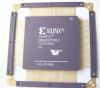
3. For protracted periods (e.g., longer than a day), VIN should not exceed VCCO by more that 3.6V.DescriptionThe XQVR1000 QPro™ Virtex™ FPGA family delivers high-performance, high-capacity programmable logic solutions. Dramatic increases in silicon efficiency result from optimizing the new architecture for place-and-route efficiency and exploiting an aggressive 5-layer-metal 0.22 µm CMOS process.
These advances make QPro Virtex FPGAs powerful and flexible alternatives to mask-programmed gate arrays. The Virtex radiation hardened family comprises the three members shown in Table 1.
Building on experience gained from previous generations of FPGAs, the Virtex family represents a revolutionary step forward in programmable logic design. Combining a wide variety of programmable system features, a rich hierarchy of fast, flexible interconnect resources, and advanced processtechnology, the QPro Virtex family delivers a high-speed and high-capacity programmable logic solution that enhances design flexibility while reducing time-to-market.
Refer to the XQVR1000"Virtex™ 2.5V Field Programmable Gate Arrays" commercial data sheet for more information on device architecture and timing specifications.

 XQVR1000 Data Sheet