Features: • 10-bit Resolution ADC• 20MHz Sampling Rate• Programmable Gain: 6dB to 38dB PGA (2x to 80x)• Improved Digitally Controlled Offset-Calibration with Pixel Averager and Hot Pixel Clipper• DNS Filter Removes Black Level Digital Noise• Widest Black Level C...
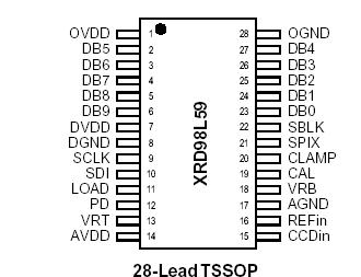
XRD98L59: Features: • 10-bit Resolution ADC• 20MHz Sampling Rate• Programmable Gain: 6dB to 38dB PGA (2x to 80x)• Improved Digitally Controlled Offset-Calibration with Pixel Averager a...
SeekIC Buyer Protection PLUS - newly updated for 2013!
268 Transactions
All payment methods are secure and covered by SeekIC Buyer Protection PLUS.
VDD to GND .......................................................... +7.0V
VRT & VRB ....................................VDD +0.5 to GND -0.5V
VIN .............................................. VDD +0.5 to GND -0.5V
All Inputs .................................... VDD +0.5 to GND -0.5V
All Outputs .................................. VDD +0.5 to GND -0.5V
Storage Temperature ............................... -65 to 150
Lead Temperature (Soldering 10 seconds) ............ 300
Maximum Junction Temperature ............................. 150
Package Power Dissipation Ratings (TA= +70)
TSSOP .........................................................JA = 90/W
ESD........................................................................ 2000V
Notes:
1 Stresses above those listed as "Absolute Maximum Ratings" may cause permanent damage to the device. This is a stress rating only and functional operation at or above this specification is not implied. Exposure to maximum rating conditions for extended periods may affect device reliability.
2 Any input pin which can see a value outside the absolute maximum ratings should be protected by Schottky diode clamps from input pin to the supplies. All inputs have protection diodes which will protect the device from short transients outside the supplies of less than 100mA for less than 100µs.
3 VDD refers to AVDD, OVDD and DVDD. GND refers to AGND, OGND and DGND.
The XRD98L59 is a complete low power CCD Image Digitizer for digital, motion and still cameras. The product includes a high bandwidth differential Correlated Double Sampler (CDS), 8-bit digitally Programmable Gain Amplifier (PGA), 10-bit Analog-to-Digital Converter (ADC) and improved digitally controlled black level auto-calibration circuitry with pixel averager hot pixel clipper, and a DNS filter.
The Correlated Double Sampler (CDS) subtracts the CCD output signal black level from the video level. Common mode signal and power supply noise are rejected by the differential CDS input stage.
The PGA is digitally controlled with 8-bit resolution on a linear dB scale, resulting in a gain range of 6dB to 38dB with 0.125dB per LSB of the gain code.
The auto calibration circuit compensates for any internal offset of the XRD98L59 as well as black level offset from the CCD.
The PGA and black level auto-calibration are controlled through a simple 3-wire serial interface. The timing circuitry is designed to enable users to select a wide variety of available CCD and image sensors for their applications.
The XRD98L59 has direct access to the ADC input for digitizing other analog signals. The XRD98L59 is packaged in 28-lead surface mount TSSOP to reduce space and weight, and is suitable for hand-held and portable applications.