Features: · 2.488 / 2.666 Gbps Transceiver
· Targeted for SONET OC-48/SDH STM-16 Applications
· Selectable full duplex operation between standard rate of 2.488 Gbps or Forward Error Correction rate of 2.666 Gbps
· Single-chip fully integrated solution containing parallel-to-serial converter, clock multiplier unit (CMU), serialto- parallel converter, and clock data recovery (CDR) functions
· 4-bit LVDS signaling data paths running at 622.08/666.51 Mbps compliant with OIF SFI-4 Implimentation Agreement
· Non-FEC and FEC rate REFCLKP/N single reference input port
· Supports 77.76/83.31 MHz or 155.52/166.63 MHz transmit and receive external reference input port
· Optional VCXO input port support multiple de-jittering modes
· On-chip phase detector and charge pump for external VCXO based de-jittering PLL
· Internal FIFO decouples transmit parallel clock input and transmit parallel clock output
· Provides Local, Remote Serial, Remote Parallel and Split Loopback modes as well as Loop Timing mode
· Diagnostics features include various lock detect functions and transmit CMU and receive CDR Lock Detect
· Host mode serial microprocessor interface simplifies monitor and control
· Meets Telcordia, ANSI and ITU-T jitter requirements including T1.105.03 - 2002 SONET Jitter Tolerance specification, GR-253 CORE, GR-253 ILR SONET Jitter specifications.
· Operates at 1.8V CMOS and CML with 3.3V I/O
· 490mW Typical Power Dissipation
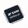
· Package: 12 x 12 mm 196-pin STBGA
· IEEE 1149.1 Compatable JTAG port
Application· SONET/SDH-based Transmission Systems
· Add/Drop Multiplexers
· Cross Connect Equipment
· ATM and Multi-Service Switches and Routers
· DSLAMS
· SONET/SDH Test Equipment
· DWDM Termination EquipmentSpecifications
| DataRate(s) |
1xOC-48, 1xSTM-16 |
| Protocols |
SONET/SDH |
| Bus I/F |
LVDS |
| SystemBus I/F |
n/a |
| Pwr Sup |
1.8V with 3.3V I/O |
| Pkgs |
STBGA-196 |
Thermal Resistance of STBGA Package....jA = 44/W
Thermal Resistance of STBGA Package....jC = 12/W
ESD Protection (HBM).......................................>2000V
Operating Temperature Range................-40 t o 85
Case Temperature under bias................-55 to 125
Storage Temperature .............................-65 to 150
Description
The XRT91L80 is a fully integrated SONET/SDHtransceiver for SONET OC-48 allowing the use ofForward Error Correction (FEC) capability. Thetransceiver includes an on-chip Clock Multiplier Unit (CMU), which uses a high frequency Phase-Locked Loop (PLL) to generate the high-speed transmit serial clock from slower external clock references. It also provides Clock and Data Recovery (CDR) functions by synchronizing its on-chip Voltage Controlled Oscillator (VCO) to the incoming serial data stream.
The chip provides serial-to-parallel and parallel-toserial converters and 4-bit LVDS system interfaces in both receive and transmit directions. The transmit section includes a 4x9 Elastic Buffer (FIFO) to absorb any phase differences between the transmitter input clock and the internally generated transmitter reference clock. In the event of an overflow, aninternal FIFO control circuit outputs an OVERFLOWindication. The FIFO under the control of the AUTORST pin can automatically recover from an overflow condition. The operation of the device can be monitored by checking the status of the LOCKDET and LOSDET output signals. An on-chip phase/frequency detector and charge-pump offers the ability to form a de-jittering PLL with an external VCXO that can be used in loop timing mode to clean up the recovered clock in the receive section.

 XRT91L80 Data Sheet


