Z8C520

Features: ` Six Vectored Interrupts with Fixed Priority` Processor Speed Dividable by Firmware Control` Operating Current: 5 mA typical in USB Mode; 2.5 mA typical in Serial Mode (@ 3 MHz); 5 mA typical in PS/2 Mode` 16 Total Input/Output Pins (Open-Drain/Push-Pull) Configurable` 6 inputs with 3 l...

product image

Z8C520 Picture
SeekIC No. : 004550446 Detail

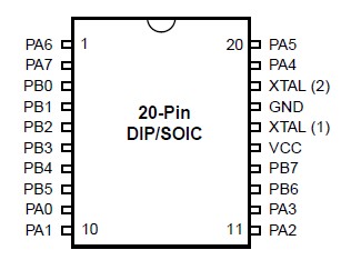
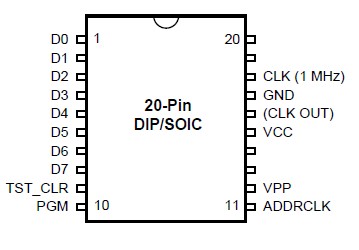
Z8C520: Features: ` Six Vectored Interrupts with Fixed Priority` Processor Speed Dividable by Firmware Control` Operating Current: 5 mA typical in USB Mode; 2.5 mA typical in Serial Mode (@ 3 MHz); 5 mA typ...

floor Price/Ceiling Price

Part Number:
Z8C520
Supply Ability:
5000

Price Break

  • Qty
  • 1~5000
  • Unit Price
  • Negotiable
  • Processing time
  • 15 Days
Total Cost: $ 0.00

SeekIC Buyer Protection PLUS - newly updated for 2013!

  • Escrow Protection.
  • Guaranteed refunds.
  • Secure payments.
  • Learn more >>

Month Sales

268 Transactions

Rating

evaluate  (4.8 stars)

Upload time: 2024/4/22

Payment Methods

All payment methods are secure and covered by SeekIC Buyer Protection PLUS.

Notice: When you place an order, your payment is made to SeekIC and not to your seller. SeekIC only pays the seller after confirming you have received your order. We will also never share your payment details with your seller.
Product Details

Description


Features:

` Six Vectored Interrupts with Fixed Priority
` Processor Speed Dividable by Firmware Control
` Operating Current: 5 mA typical in USB Mode; 2.5 mA typical in Serial Mode (@ 3 MHz); 5 mA typical in PS/2 Mode
` 16 Total Input/Output Pins (Open-Drain/Push-Pull) Configurable
` 6 inputs with 3 level Programmable Reference Comparators
` 16-Bit Programmable Watch-Dog Timer (WDT) with Internal RC Oscillator
` Software Programmable Timers Configurable as:
Two 8-Bit Standard Timers and One 16-Bit Standard Timer or
One 16-Bit Standard Timer and One 16-Bit Pulse Width Modulator (PWM) Timer
` Identical Masked ROM Version (Z8C520)
` On-Chip Oscillator that accepts a Ceramic Resonator or External Clock
` Hardware Support for PS/2, Serial, USB, and General-Purpose I/O (GPIO)
` Power Reduction Modes:
STOP Mode (functionality shut down except SMR)
HALT Mode (XTAL still running-peripherals active)
` USB SIE Compliant with USB Spec 1.0
` 4.0 VDC to 6.0 VDC Operating Range @ 0 to +70


Pinout

  Connection Diagram


  Connection Diagram


Specifications

Parameter Min Max Units Note
Ambient Temperature under Bias 40 +105 C  
Storage Temperature 65 +150 C  
Voltage on any Pin with Respect to VSS 0.6 +7 V  
Voltage on VDD Pin with Respect to VSS 0.3 +7 V  
Total Power Dissipation   880 mW  
Maximum Allowable Current out of VSS   80 mA  
Maximum Allowable Current into VDD   80 mA  
Maximum Allowable Current into an Input Pin 600 +600 A 1
Maximum Allowable Current into an Open-Drain Pin 600 +600 A 2
Maximum Allowable Sink Output Current by Any I/O Pin   25 mA  
Maximum Allowable Source Output Current by Any I/O Pin   25 mA  
Maximum Allowable Sink Output Current by Port A   40 mA  
Maximum Allowable Source Output Current by Port A   40 mA  
Maximum Allowable Sink Output Current by Port B   40 mA  
Maximum Allowable Source Output Current by Port B   40 mA  

Notes:
1. Excludes XTAL pins.
2. Device pin is not at an output Low state.


Description

Zilog's Z8E520 (OTP) and Z8C520 (Masked ROM) microcontrollers are low-power Z8Plus MCUs, designed for the cost-effective implementation of USB and multiprotocol pointing devices.

For applications demanding powerful I/O capabilities, the Z8E520's input and output lines are grouped into two ports, and are configurable under software control to provide timing, status signals, or parallel I/O.

Both 8-bit and 16-bit timers, with a large number of user selectable modes, off-load the system of administering realtime tasks such as counting/timing and I/O data communications.

The microcontroller clock frequency is derived from the system clock by a programmable divider under firmware control.

The device is capable of functioning in four distinct, selectable communications modes: PS/2, RS232, GPIO (General- purpose I/O), and USB. The communications mode determines the functionality of the two special serial communications pins (PB6 and PB7). The device is placed in the required mode when firmware sets the specified mode bit in the communications control register. The firmware interface is similar in all modes. The same buffer area in RAM will accept the data to be transmitted. Up to 8 bytes may be loaded, and the data will actually be transmitted as soon as the appropriate command is issued (setting In Packet Ready in USB mode, for example).


Customers Who Bought This Item Also Bought

Margin,quality,low-cost products with low minimum orders. Secure your online payments with SeekIC Buyer Protection.
LED Products
Circuit Protection
Batteries, Chargers, Holders
Line Protection, Backups
Fans, Thermal Management
View more