Features: • All Instructions Execute in one 1-s Instruction Cycle with a 10-MHz Crystal
• 1K x 8 On-Chip OTP EPROM Memory
• 64 x 8 General-Purpose Registers (SRAM)
• Six Vectored Interrupts with Fixed Priority
• Operating Speed: DC10 MHz
• Six Addressing Modes:R, IR, X, D, RA, and IM
ApplicationThe Z8PE003 is the newest member of the Z8Plus Microprocessor (MPU) family. Similar to the Z8E000 and Z8E001, the Z8PE003 offers easy software development, debug, prototyping, and an attractive One-Time Programmable (OTP) solution.
For applications demanding powerful I/O capabilities, the Z8PE003's dedicated input and output lines are grouped into two ports, and are configurable under software control.
Pinout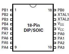 Specifications
|
Parameter |
Min |
Max |
Units |
Note |
| Ambient Temperature under Bias |
-40 |
+105 |
C |
|
| Storage Temperature |
-65 |
+150 |
C |
|
| Voltage on any Pin with Respect to VSS |
-0.6 |
+7 |
V |
1 |
| Voltage on VDD Pin with Respect to VSS |
0.3 |
+7 |
V |
|
| Voltage on PB5 Pin with Respect to VSS |
0.6 |
VDD+1 |
V |
2 |
| Total Power Dissipation |
|
880 |
mW |
|
| Maximum Allowable Current out of VSS |
|
40 |
mW |
3 |
| Maximum Allowable Current into VDD |
|
40 |
mW |
3 |
| Maximum Allowable Current into an Input Pin |
600 |
+600 |
A |
4 |
| Maximum Allowable Current into an Open-Drain Pin |
600 |
+600 |
A |
5 |
| Maximum Allowable Output Current Sunk by Any I/O Pin |
|
25 |
mA |
|
| Maximum Allowable Output Current Sourced by Any I/O Pin |
|
25 |
mA |
|
| Maximum Allowable Output Current Sunk by Port A |
|
40 |
mA |
3 |
| Maximum Allowable Output Current Sourced by Port A |
|
40 |
mA |
3 |
| Maximum Allowable Output Current Sunk by Port B |
|
40 |
mA |
3 |
| Maximum Allowable Output Current Sourced by Port B |
|
40 |
mA |
3 |
Notes:
1. Applies to all pins except the PB5 pin and where otherwise noted.
2. There is no input protection diode from pin to VDD.
3. Peak Current. Do not exceed 25mA average current in either direction.
4. Excludes XTAL pins.
5. Device pin is not at an output Low state.Description• 14 Total Input/Output Pins
• One 8-Bit I/O Port (Port A) I/O Bit Programmable Each Bit Programmable as Push-Pull or Open-Drain
• One 6-Bit I/O Port (Port B) I/O Bit Programmable Includes Special Functionality: Stop-Mode Recovery Input, Comparator Inputs, Selectable Edge Interrupts, and Timer Output
• One Analog Comparator

 Z8PE003 Data Sheet


