Features: • Output Frequency up to 125MHz
• Supports Power PC TM, and Pentium TM Processors
• 15 Clock Output: Frequency Configurable
• Two Reference Clock Inputs for Dynamic Toggling
• Output Tri-State Control
• Spread Spectrum Compatible
• 3.3V Power Supply
• Pin Compatible with MPC974
• Industrial Temp. Range: -40°C to +85°C
• 52 Pin TQFP PackagePinout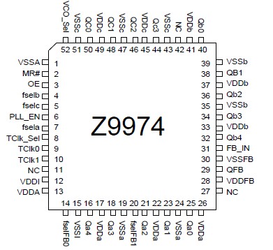 Specifications
Input Voltage Relative to VSS: ........VSS-0.3V
Input Voltage Relative to VDD........ VDD+0.3V
Storage Temperature: .......-65°C to + 150°C
Operating Temperature:....... -40°C to +85°C
Maximum Power Supply:.............. 5.5V
This device contains circuitry to protect the inputs against damage due to high static voltages or electric field; however, precautions should be taken to avoid application of any voltage higher than the maximum rated voltages to this circuit. For proper operation, Vin and Vout should be constrained to the range: VSS<(Vin or Vout)<VDD
Unused inputs must always be tied to an appropriate logic voltage level (either VSS or VDD).
Description
The Z9974 is a low cost 3.3V zero delay clock driver for high speed signal buffering and redistribution.
It provides the designer with the flexibility of selecting various Output/Input Frequency ratios selected by fsela, fselb, fselc, fselFB(0:1), and VCO_sel input settings.
The Z9974 integrates PLL technology for Zero delay propagation from Input to Output. The PLL feedback is externally available for propagation delay tuning and divide ratio alternatives as per table 1.
The Z9974 has three banks of outputs with independent divider stages. These dividers allow the banks to have different frequencies as per table 2.
TCLK0 and TCLK1 one are selectable input reference clocks and may be toggled dynamically during operation to provide modulation and phase shifting designs.
This device includes a Master Reset signal, which disables the outputs into Tristate (Hi-Z) mode, and reset all internal digital circuitry (excluding the PLL).
An Output Enable, OE, input pin is available for shutting Qa(0:4), Qb(0:4), and Qc(0:3) outputs in a low state. All outputs are held low with input clock turned off.

 Z9974 Data Sheet


