Features: Members of the Texas Instruments
Widebus Family
Inputs Are TTL-Voltage Compatible
Independent Registers for A and B Buses
Multiplexed Real-Time and Stored Data
Flow-Through Architecture Optimizes
PCB Layout
Distributed VCC and GND Pin Configuration
Minimizes High-Speed Switching Noise
EPIC (Enhanced-Performance Implanted
CMOS) 1-m Process
500-mA Typical Latch-Up Immunity at
125°C
Package Options Include Plastic 300-mil
Shrink Small-Outline (DL) Packages Using
25-mil Center-to-Center Pin Spacings and
380-mil Fine-Pitch Ceramic Flat (WD)
Packages Using 25-mil Center-to-Center
Pin SpacingsPinout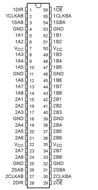 SpecificationsSupply voltage range, VCC . . . . . . . . . . . . . . . . . . . . . . . . . . . . . . . . . . . . . . . . . . . . ... 0.5 V to 7 V
Input voltage range, VI (see Note 1) . . . . . . . . . . . . . . . . . . . . . . . . . . . . . . . 0.5 V to VCC + 0.5 V
Output voltage range, VO (see Note 1) . . . . . . . . . . . . . . . . . . . . . . . . . . . .... 0.5 V to VCC + 0.5 V
Input clamp current, IIK (VI < 0 or VI > VCC ) . . . . ... . . . . . . . . . . . . . . . . . . . . . . . . . .. .. . . ±20 mA
Output clamp current, IOK (VO < 0 or VO > VCC ) . . . . .. . . . . . . . . . . . . . . . . . . .. .. . . . . . . ± 50 mA
Continuous output current, IO (VO = 0 to VCC ) . . . . . . . . . . . . . . . . . . . . . . . . . . .. . . . . . . . ± 50 mA
Continuous current through VCC or GND . . . . . . . . . . . . . . . . . . . . . .. . . . . . . . . . . . . . . . . ± 400 mA
Maximum package power dissipation at TA = 55 (in still air) (see Note 2): DL package . . . . .1.4 W
Storage temperature range, Tstg . . . . . . . . . . . . . . . . . . . . . . . . . . . . . . . . . .......... . .. 65 to 150
DescriptionThe 74ACT16646 are 16-bit bus transceivers consisting of D-type flip-flops and control circuitry with 3-state outputs arranged for multiplexed transmission of data directly from the data bus or from the internal storage registers. The devices can be used as two 8-bit transceivers or one 16-bit transceiver. Data on the A or B bus is clocked into the registers on the low-to-high transition of the appropriate clock (CLKAB or CLKBA) input. Figure 1 illustrates the four fundamental bus- management functions that can be performed with the bus transceivers and registers.
Output-enable (OE) and direction-control (DIR) inputs of the 74ACT16646 are provided to control the transceiver functions. In the transceiver mode, data present at the high-impedance port may be stored in either register or in both. The select controls (SAB and SBA) can multiplex stored and real-time (transparent mode) data. The circuitry used for select control eliminates the typical decoding glitch that occurs in a multiplexer during the transition between stored and real-time data. DIR determines which bus receives data when OE is low. In the isolation mode (OE high), A data may be stored in one register and/or B data may be stored in the other register.
When an output function is disabled, the input function of the 74ACT16646 is still enabled and may be used to store and transmit data. Only one of the two buses, A or B, may be driven at a time.
The 74ACT16646 is packaged in TI's shrink small-outline package, which provides twice the functionality of standard small-outline packages in the same printed-circuit-board area.
The 54ACT16646 is characterized for operation over the full military temperature range of 55°C to 125°C. The 74ACT16646 is characterized for operation from 40°C to 85°C.

 74ACT16646 Data Sheet