PLL102-108

Features: ` PLL clock distribution optimized for Double Data Rate SDRAM application up to 266Mhz. ` Distributes one clock Input to one bank of ten differential outputs. ` Track spread spectrum clocking for EMI reduction. ` Programmable delay between CLK_INT and CLK[T/C] from 0.8ns to +3.1ns by pro...

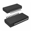
product image

PLL102-108 Picture
SeekIC No. : 004463298 Detail

PLL102-108: Features: ` PLL clock distribution optimized for Double Data Rate SDRAM application up to 266Mhz. ` Distributes one clock Input to one bank of ten differential outputs. ` Track spread spectrum clock...

floor Price/Ceiling Price

Part Number:
PLL102-108
Supply Ability:
5000

Price Break

  • Qty
  • 1~5000
  • Unit Price
  • Negotiable
  • Processing time
  • 15 Days
Total Cost: $ 0.00

SeekIC Buyer Protection PLUS - newly updated for 2013!

  • Escrow Protection.
  • Guaranteed refunds.
  • Secure payments.
  • Learn more >>

Month Sales

268 Transactions

Rating

evaluate  (4.8 stars)

Upload time: 2024/4/27

Payment Methods

All payment methods are secure and covered by SeekIC Buyer Protection PLUS.

Notice: When you place an order, your payment is made to SeekIC and not to your seller. SeekIC only pays the seller after confirming you have received your order. We will also never share your payment details with your seller.
Product Details

Description


Features:

`  PLL clock distribution optimized for Double Data Rate SDRAM application up to 266Mhz.
`  Distributes one clock Input to one bank of ten differential outputs.
`  Track spread spectrum clocking for EMI reduction.
`  Programmable delay between CLK_INT and CLK[T/C] from 0.8ns to +3.1ns by programming CLKINT and FBOUT skew channel, or from 1.1ns to +3.5ns if additional DDR skew channels are enabled.
`  Four independent programmable DDR skew chan-nels from 0.3ns to +0.4ns with step size ±100ps.
`  Support 2-wire I2C serial bus interface.  
`  2.5V Operating Voltage.
`  Available in 48-Pin 300mil SSOP.


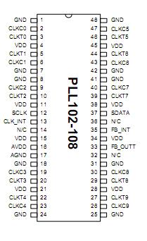
Pinout

  Connection Diagram


Specifications

SYMBOL PARAMETERS MIN. MAX. UNITS
VCC Supply Voltage Range -0.5 3.6 V
VI Input Voltage Range -0.5 VCC+0.5 V
VO Output Voltage Range -0.5 VCC+0.5 V
TS Storage Temperature -65 150
PW Maximum power dissipation at TA = 550C in still air   0.7 W

Exposure of the device under conditions beyond the limits specified by Maximum Ratings for extended periods may cause permanent damage to the  device and affect product reliability.  These conditions represent a stress rating only, and functional operations of the device at these or any other con-ditions above the operational limits noted in this specification is not implied.


Description

The PLL102-108 is a zero delay buffer that distributes a single-ended clock input to ten pairs of differential clock outputs and one feedback clock output. Output signal duty cycles are adjusted to 50%, independent of the duty cycle at CLK_INT. The  PLL102-108 PLL can be bypassed  for test purposes by strapping AVdd to ground.


Customers Who Bought This Item Also Bought

Margin,quality,low-cost products with low minimum orders. Secure your online payments with SeekIC Buyer Protection.
Hardware, Fasteners, Accessories
Static Control, ESD, Clean Room Products
Power Supplies - External/Internal (Off-Board)
Sensors, Transducers
Memory Cards, Modules
Transformers
View more