Features: ·Convert TTL Voltage Levels to MOS Levels
·High Sink-Current Capability
·Input Clamping Diodes Simplify System Design
·Open-Collector Driver for Indicator Lamps and Relays
·Inputs Fully Compatible With Most TTL CircuitsPinout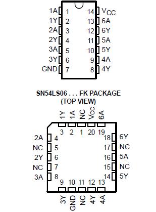 Specifications
Supply voltage, VCC . . . . . . . . . . . . . . . . . . . . . . . . . . . . . .. . . . . . . 7 V
Input voltage, VI (see Note 1) . . . . . . . . . . . . . . . . . . . . . . . . . . . 5.5 V
Output voltage, VO (see Notes 1 and 2): SN54LS06, SN74LS06 . . 30 V
SN74LS16 . . . . . . . . . . . . . . . . . . . . . . . . . . . . . . . . . . . . . . . . . . . 15 V
Package thermal impedance, JA (see Note 3): D package . . .86°C/W
N package . . . . . . . . . . . . . . . . . . . . . . . . . . . .. . . . . . . . . . . . 80°C/W
NS package . . . . . . . . . . . . . . . . .. . . . . . . . . . . . . . . . . . . . . . 76°C/W
Storage temperature range, Tstg . . . . . . . . . . . . .. . 65°C to 150°C
† Stresses beyond those listed under "absolute maximum ratings" may cause permanent damage to the device. These are stress ratings only, and functional operation of the device at these or any other conditions beyond those indicated under "recommended operating conditions" is not implied. Exposure to absolute-maximum-rated conditions for extended periods may affect device reliability.
NOTES: 1. All voltage values are with respect to GND.
2. This is the maximum voltage that should be applied to any output when it is in the off state.
3. The package thermal impedance is calculated in accordance with JESD 51-7.
DescriptionThese hex inverter buffers/drivers feature high-voltage open-collector outputs to interface with high-level circuits (such as MOS), or for driving high-current loads, and also are characterized for use as inverter buffers for driving TTL inputs. The 'LS06 devices have a rated output voltage of 30 V, and the SN74LS16 has a rated output voltage of 15 V. The maximum sink current for the SN54LS06 is 30 mA, and for the SN74LS06 and SN74LS16 is 40 mA.
These devices of the SN74LS16 are compatible with most TTL families. Inputs are diode-clamped to minimize transmission effects, which simplifies design. Typical power dissipation is 175 mW and average propagation delay time is 8 ns.

 SN74LS16 Data Sheet


