Features: • ComboMemories organized as: SST32HF1621C: 1M x16 Flash + 128K x16 SRAM SST32HF1641x: 1M x16 Flash + 256K x16 SRAM SST32HF1681: 1M x16 Flash + 256K x16 SRAM SST32HF3241x: 2M x16 Flash + 256K x16 SRAM SST32HF3281: 2M x16 Flash + 512K x16 SRAM• Single 2.7-3.3V Read and Write O...
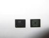
SST32HF1641C: Features: • ComboMemories organized as: SST32HF1621C: 1M x16 Flash + 128K x16 SRAM SST32HF1641x: 1M x16 Flash + 256K x16 SRAM SST32HF1681: 1M x16 Flash + 256K x16 SRAM SST32HF3241x: 2M x16 Fla...
SeekIC Buyer Protection PLUS - newly updated for 2013!
268 Transactions
All payment methods are secure and covered by SeekIC Buyer Protection PLUS.
The SST32HF1641C ComboMemory devices integrate a CMOS flash memory bank with a CMOS SRAM memory bank in a Multi-Chip Package (MCP), manufactured with SST's proprietary, high performance SuperFlash technology. The SST32HF16x1/32x1 devices use a PseudoSRAM. The SST32HF16x1C/32x1C devices use standard SRAM.
Featuring high performance Word-Program, the flash memory bank provides a maximum Word-Program time of 7 sec. To protect against inadvertent flash write, the SST32HFx1/x1C devices contain on-chip hardware and software data protection schemes. The SST32HFx1/x1C devices offer a guaranteed endurance of 10,000 cycles. Data retention is rated at greater than 100 years.
The SST32HF1641C devices consist of two independent memory banks with respective bank enable signals. The Flash and SRAM memory banks are superimposed in the same memory address space. Both memory banks share common address lines, data lines, WE# and OE#. The memory bank selection is done by memory bank enable signals. The SRAM bank enable signal, BES# selects the SRAM bank. The flash memory bank enable signal, BEF# selects the flash memory bank. The WE# signal has to be used with Software Data Protection (SDP) command sequence when controlling the Erase and Program operations in the flash memory bank. The SDP command sequence protects the data stored in the flash memory bank from accidental alteration.
The SST32HF1641C provide the added functionality of being able to simultaneously read from or write to the SRAM bank while erasing or programming in the flash memory bank. The SRAM memory bank can be read or written while the flash memory bank performs Sector- Erase, Bank-Erase, or Word-Program concurrently. All flash memory Erase and Program operations will automatically latch the input address and data signals and complete the operation in background without further input stimulus requirement. Once the internally controlled Erase or Program cycle in the flash bank has commenced, the SRAM bank can be accessed for Read or Write.