Features: ` Self-Calibrates Input Offset Voltage to 40 mV Max
` Low Input Offset Voltage Drift . . . 1 mV/
` Input Bias Current . . . 1 pA
` Open Loop Gain . . . 120 dB
` Rail-To-Rail Output Voltage Swing
` Stable Driving 1000 pF Capacitive Loads
` Gain Bandwidth Product . . . 4.7 MHz
` Slew Rate . . . 2.5 V/ms
` High Output Drive Capability . . . ±50 mA
` Calibration Time . . . 300 ms
` Characterized From 55 to 125
` Available in Q-Temp Automotive
HighRel Automotive Applications
Configuration Control / Print Support
Qualification to Automotive Standards
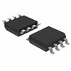
Pinout Specifications
Supply voltage, VDD+ (see Note 1) . . . . . . . . . . . . . . . . . . . . . . . . . . . . . . . . 7 V
Differential input voltage, VID (see Note 2) . . . . . . . . . . . . . . . . . . . . .. . . . ±7 V
Input voltage range, VI (any input, see Note 1) . . . . . . . . . . . . . . 0.3 V to 7 V
Input current, II (each input) . . . . . . . . . . . . . . . . . . . . . . . . . . . . . . . . . . ±5 mA
Output current, IO (each output) . . . . . . . . . . . . . . . . . . . . . . . . . . . . . ±100 mA
Total current into VDD+ . . . . . . . . . . . . . . . . . . . . . . . . . . . . . . . . . . . . ±100 mA
Total current out of VDD/GND . . . . . . . . . . . . . . . . . . . . . . . . . . . . . . . ±100 mA
Electrostatic discharge (ESD) . . . . . . . . . . . . . . . . . . . . . . .. . . . . . . . . . . > 2 kV
Duration of short-circuit current at (or below) 25 (see Note 3) .. . . . unlimited
Continuous total power dissipation . . . . . . . . . . . . See Dissipation Rating Table
Operating free-air temperature range, TA: TLC4502C .. . .. . .. . .. . . . 0 to 70
TLC4502I . . . . . . . . . . . . . . . . . . . . . . . . . . ... . .. . .. . .. . . . . . . . . 40 to 125
TLC4502Q . . . . . . . . . . . . . . . . . . . . . . . . . . ... . .. . .. . .. . . . . . . . 40 to 125
TLC4502M . . . . . . . . . . . . . . . . . . . . . ... . .. . .. . .. . . . . . . . . . . . . 55 to 125
Storage temperature range, Tstg . . . . . . . . . . . . . .. . . . . . . . . . . . 65 to 150
Case temperature for 60 seconds, TC: FK package . . . . . . . . . . . . . . . . . . 260
Lead temperature 1,6 mm (1/16 inch) from case for 10 seconds . . . . . ... . 260
† Stresses beyond those listed under "absolute maximum ratings" may cause permanent damage to the device. These are stress ratings only, and functional operation of the device at these or any other conditions beyond those indicated under "recommended operating conditions" is not implied. Exposure to absolute-maximum-rated conditions for extended periods may affect device reliability.
NOTES: 1. All voltage values, except differential voltages, are with respect to VDD /GND.
2. Differential voltages are at IN+ with respect to IN . Excessive current flows when an input is brought below VDD 0.3 V.
3. The output may be shorted to either supply. Temperature and/or supply voltages must be limited to ensure that the maximum dissipation rating is not exceeded.
DescriptionThe TLC4501 and TLC4502 are the highest precision CMOS single supply rail-to-rail operational amplifiers available today. The input offset voltage is 10 mV typical and 40 mV maximum. This exceptional precision, combined with a 4.7-MHz bandwidth, 2.5-V/ms slew rate, and 50-mA output drive, is ideal for multiple applications including: data acquisition systems, measurement equipment, industrial control applications, and portable digital scales.
These amplifiers TLC4501 feature self-calibrating circuitry which digitally trims the input offset voltage to less than 40 mV within the first 300 ms of operation. The offset is then digitally stored in an integrated successive approximation register (SAR). Immediately after the data is stored, the calibration circuitry of TLC4501 effectively drops out of the signal path, shuts down, and the device functions as a standard operational amplifier.

 TLC4501 Data Sheet