dsPIC33F

Features: dsPIC33F devices include several features intended to maximize application flexibility and reliability, and minimize cost through elimination of external components. These are:• Flexible Configuration• Watchdog Timer (WDT)• Code Protection• JTAG Boundary Scan Inte...

product image

dsPIC33F Picture
SeekIC No. : 004329695 Detail

dsPIC33F: Features: dsPIC33F devices include several features intended to maximize application flexibility and reliability, and minimize cost through elimination of external components. These are:• Flex...
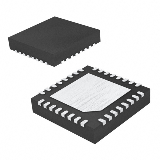
floor Price/Ceiling Price

Part Number:
dsPIC33F
Supply Ability:
5000

Price Break

  • Qty
  • 1~5000
  • Unit Price
  • Negotiable
  • Processing time
  • 15 Days
Total Cost: $ 0.00

SeekIC Buyer Protection PLUS - newly updated for 2013!

  • Escrow Protection.
  • Guaranteed refunds.
  • Secure payments.
  • Learn more >>

Month Sales

268 Transactions

Rating

evaluate  (4.8 stars)

Upload time: 2024/4/28

Payment Methods

All payment methods are secure and covered by SeekIC Buyer Protection PLUS.

Notice: When you place an order, your payment is made to SeekIC and not to your seller. SeekIC only pays the seller after confirming you have received your order. We will also never share your payment details with your seller.
Product Details

Description


Features:

dsPIC33F devices include several features intended to maximize application flexibility and reliability, and minimize cost through elimination of external components. These are:
• Flexible Configuration
• Watchdog Timer (WDT)
• Code Protection
• JTAG Boundary Scan Interface
• In-Circuit Serial Programming™ (ICSP™)
• In-Circuit Emulation


Specifications

Absolute Maximum Ratings(†)
Ambient temperature under bias................................................................................. .-40°C to +85°C
Storage temperature ................................................................................................. -65°C to +150°C
Voltage on VDD with respect to VSS ................................................................................. -0.3V to +4.0V
Voltage on any combined analog and digital pin and MCLR, with respect to VSS.... -0.3V to (VDD + 0.3V)
Voltage on any digital-only pin with respect to VSS ........................................................... -0.3V to +5.6V
Voltage on VDDCORE with respect to VSS ......................................................................... 2.25V to 2.75V
Maximum current out of VSS pin ....................................................................................................300 mA
Maximum current into VDD pin (Note 1)...........................................................................................250 mA
Maximum output current sunk by any I/O pin.....................................................................................4 mA
Maximum output current sourced by any I/O pin ................................................................................4 mA
Maximum current sunk by all ports .................................................................................................200 mA
Maximum current sourced by all ports (Note 1)...............................................................................200 mA

Note 1: Maximum allowable current is a function of device maximum power dissipation (see Table 27-2).

†NOTICE: Stresses above those listed under "Absolute Maximum Ratings" may cause permanent damage to the
device. This is a stress rating only and functional operation of the device at those or any other conditions above those
indicated in the operation listings of this specification is not implied. Exposure to maximum rating conditions for
extended periods may affect device reliability.


Customers Who Bought This Item Also Bought

Margin,quality,low-cost products with low minimum orders. Secure your online payments with SeekIC Buyer Protection.
Cables, Wires
Computers, Office - Components, Accessories
Transformers
Potentiometers, Variable Resistors
Test Equipment
Undefined Category
View more