gm5120-H

Features: • Zoom (from VGA) and shrink (from UXGA) scaling• Integrated 8-bit triple-channel ADC / PLL• Integrated Ultra-Reliable DVI™ 1.0-compliant receiver• High-Bandwidth Digital Content Protection (HDCP)• Embedded microcontroller with parallel ROM interface&#...

product image

gm5120-H Picture
SeekIC No. : 004354112 Detail

gm5120-H: Features: • Zoom (from VGA) and shrink (from UXGA) scaling• Integrated 8-bit triple-channel ADC / PLL• Integrated Ultra-Reliable DVI™ 1.0-compliant receiver• High-Bandw...

floor Price/Ceiling Price

Part Number:
gm5120-H
Supply Ability:
5000

Price Break

  • Qty
  • 1~5000
  • Unit Price
  • Negotiable
  • Processing time
  • 15 Days
Total Cost: $ 0.00

SeekIC Buyer Protection PLUS - newly updated for 2013!

  • Escrow Protection.
  • Guaranteed refunds.
  • Secure payments.
  • Learn more >>

Month Sales

268 Transactions

Rating

evaluate  (4.8 stars)

Upload time: 2024/4/27

Payment Methods

All payment methods are secure and covered by SeekIC Buyer Protection PLUS.

Notice: When you place an order, your payment is made to SeekIC and not to your seller. SeekIC only pays the seller after confirming you have received your order. We will also never share your payment details with your seller.
Product Details

Description


Features:

• Zoom (from VGA) and shrink (from UXGA) scaling
• Integrated 8-bit triple-channel ADC / PLL
• Integrated Ultra-Reliable DVI™ 1.0-compliant receiver
• High-Bandwidth Digital Content Protection (HDCP)
• Embedded microcontroller with parallel ROM interface
• On-chip versatile OSD engine
• All system clocks synthesized from a single external crystal
• Programmable gamma correction (CLUT)
• RealColor controls provide sRGB compliance
• PWM back light intensity control
• 5-Volt tolerant inputs
• Low EMI and power saving features


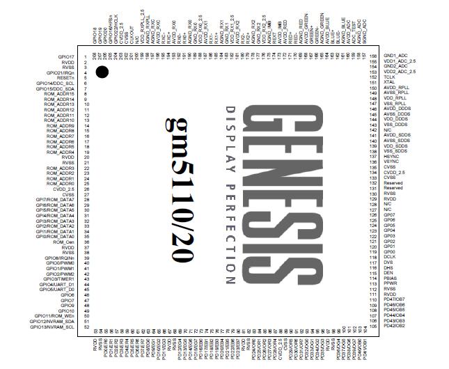
Pinout

  Connection Diagram


Specifications

PARAMETER SYMBOL MIN TYP MAX UNITS
3.3V Supply Voltages (1,2) VVDD_3.3 -0.3   3.6 V
2.5V Supply Voltages (1.2) VVDD_2.5 -0.3   2.75 V
Input Voltage (5V tolerant inputs) (1,2) VIN5Vtol -0.3   5.5 V
Input Voltage (non 5V tolerant inputs) (1,2) VIN -0.3   3.6 V
Electrostatic Discharge VESD     ±2.0 kV
Latch-up ILA     ±100 mA
Ambient Operating Temperature TA 0   70
Storage Temperature TSTG -40   125
Operating Junction Temp. TJ 0   125
Thermal Resistance (Junction to Air) Natural Convection (3)
gm5110
gm5120
JA_5110
JA_5120
    32.4
22.0
/W
Thermal Resistance (Junction to Case) Convection (4)
gm5110
gm5120
JC_5110
JC_5120
    13.9
10.1
/W
Soldering Temperature (30 sec.) TSOL     220
Vapor Phase Soldering (30 sec.) TVAP     220


Description

A functional block diagram of gm5110/20 is illustrated below. Each of the functional units shown is described in the following sections.

The gm5110/20 features three clock inputs. All additional clocks are internal clocks derived from one or more of these:

1. Crystal Input Clock (TCLK and XTAL). This is the input pair to an internal crystal oscillator and corresponding logic. A 14.3 MHz TV crystal is recommended. Other crystal frequencies may be used, but require custom programming. This is illustrated in Figure 4 below.

Alternatively, a single-ended TTL/CMOS clock oscillator can be driven into the TCLK pin (leave XTAL as N/C in this case). This is illustrated in Figure 7 below. This option is selected by connecting a 10K pull-up to ROM_ADDR13 (refer to Table 18). See also Table 14.

2. DVI Differential Input Clock (RC+ and RC-)

3. Host Interface Transfer Clock (HCLK)

The gm5110/20 TCLK oscillator circuitry is a custom designed circuit to support the use of an external oscillator or a crystal resonator to generate a reference frequency source for the gm5110/20 device.


Customers Who Bought This Item Also Bought

Margin,quality,low-cost products with low minimum orders. Secure your online payments with SeekIC Buyer Protection.
Undefined Category
Power Supplies - External/Internal (Off-Board)
Sensors, Transducers
LED Products
Cables, Wires
View more