ispLSI2032VE

Features: * SuperFAST HIGH DENSITY IN-SYSTEM PROGRAMMABLE LOGIC - 1000 PLD Gates - 32 I/O Pins, Two Dedicated Inputs - 32 Registers - High Speed Global Interconnect - Wide Input Gating for Fast Counters, State Machines, Address Decoders, etc. - Small Logic Block Size for Random Logic - 100% Functi...

product image

ispLSI2032VE Picture
SeekIC No. : 004381215 Detail

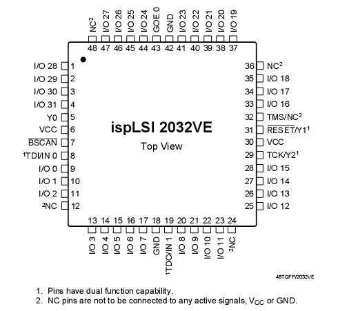
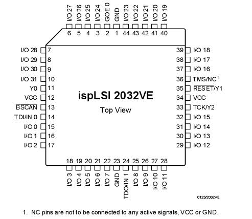
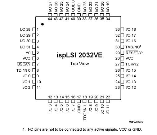
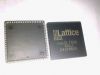
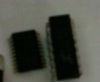
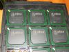
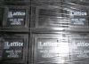
ispLSI2032VE: Features: * SuperFAST HIGH DENSITY IN-SYSTEM PROGRAMMABLE LOGIC - 1000 PLD Gates - 32 I/O Pins, Two Dedicated Inputs - 32 Registers - High Speed Global Interconnect - Wide Input Gating for Fast Coun...

floor Price/Ceiling Price

Part Number:
ispLSI2032VE
Supply Ability:
5000

Price Break

  • Qty
  • 1~5000
  • Unit Price
  • Negotiable
  • Processing time
  • 15 Days
Total Cost: $ 0.00

SeekIC Buyer Protection PLUS - newly updated for 2013!

  • Escrow Protection.
  • Guaranteed refunds.
  • Secure payments.
  • Learn more >>

Month Sales

268 Transactions

Rating

evaluate  (4.8 stars)

Upload time: 2024/5/3

Payment Methods

All payment methods are secure and covered by SeekIC Buyer Protection PLUS.

Notice: When you place an order, your payment is made to SeekIC and not to your seller. SeekIC only pays the seller after confirming you have received your order. We will also never share your payment details with your seller.
Product Details

Description


Features:

* SuperFAST HIGH DENSITY IN-SYSTEM PROGRAMMABLE LOGIC
   - 1000 PLD Gates
   - 32 I/O Pins, Two Dedicated Inputs
   - 32 Registers
   - High Speed Global Interconnect
   - Wide Input Gating for Fast Counters, State Machines, Address Decoders, etc.
   - Small Logic Block Size for Random Logic
   - 100% Functional, JEDEC and Pinout Compatible with ispLSI 2032V Devices
* 3.3V LOW VOLTAGE 2032 ARCHITECTURE
  - Interfaces With Standard 5V TTL Devices
* HIGH PERFORMANCE E2CMOS(R)TECHNOLOGY
   - fmax = 225 MHz Maximum Operating Frequency
   - tpd = 4.0 ns Propagation Delay
   - Electrically Erasable and Reprogrammable
   - Non-Volatile
   - 100% Tested at Time of Manufacture
   - Unused Product Term Shutdown Saves Power
* IN-SYSTEM PROGRAMMABLE
  - 3.3V In-System Programmability Using Boundary Scan Test Access Port (TAP)
  - Open-Drain Output Option for Flexible Bus Interface Capability, Allowing Easy Implementation of Wired-OR or Bus Arbitration Logic
  - Increased Manufacturing Yields, Reduced Time-to-Market and Improved Product Quality
  - Reprogram Soldered Devices for Faster Prototyping
* 100% IEEE 1149.1 BOUNDARY SCAN TESTABLE
* THE EASE OF USE AND FAST SYSTEM SPEED OF PLDs WITH THE DENSITY AND FLEXIBILITY OF FPGAs
   - Enhanced Pin Locking Capability
   - Three Dedicated Clock Input Pins
   - Synchronous and Asynchronous Clocks
   - Programmable Output Slew Rate Control
   - Flexible Pin Placement
   - Optimized Global Routing Pool Provides Global Interconnectivity
* ispDesignEXPERT(TM) LOGIC COMPILER AND COM-PLETE ISP DEVICE DESIGN SYSTEMS FROM HDL SYNTHESIS THROUGH IN-SYSTEM PROGRAMMING
   - Superior Quality of Results
   - Tightly Integrated with Leading CAE Vendor Tools
   - Productivity Enhancing Timing Analyzer, Explore Tools, Timing Simulator and ispANALYZER(TM)
   - PC and UNIX Platforms


Pinout

  Connection Diagram  Connection Diagram  Connection Diagram


Specifications

Supply Voltage Vcc .................................. -0.5 to +5.4V
Input Voltage Applied............................... -0.5 to +5.6V
Off-State Output Voltage Applied ............ -0.5 to +5.6V
Storage Temperature..............................-65 to +150
Case Temp. with Power Applied ..............-55 to 125
Max. Junction Temp. (TJ) with Power Applied ... 150
1. Stresses above  those listed  under  the "Absolute  Maximum Ratings" may cause permanent damage to the device. Functional operation of the device at these or at any other conditions above those indicated in the operational sections of this specification is not implied (while programming, follow the programming specifications).


Description

The ispLSI 2032VE is a High Density Programmable Logic Device that can be used in both 3.3V and 5V systems.  The device contains 32 Registers, 32 Universal I/O pins, two Dedicated Input Pins, three Dedicated Clock Input Pins, one dedicated Global OE input pin and a Global Routing  Pool (GRP).  The GRP provides complete interconnectivity between all of these elements.The ispLSI 2032VE features in-system programmability through the Boundary Scan Test Access Port (TAP) and is 100% IEEE 1149.1 Boundary Scan Testable.  The ispLSI 2032VE offers non-volatile reprogrammability of
the logic, as well as the interconnect to provide truly reconfigurable systems.
The basic unit of logic on the ispLSI 2032VE device is the Generic Logic Block (GLB). The GLBs are labeled A0, A1.. A7 (see Figure 1).  There are a total of eight GLBs in the ispLSI 2032VE device. Each GLB is made up of four macrocells.  Each GLB has 18 inputs, a programmable AND/OR/Exclusive OR array, and four outputs which can be configured to be either combinatorial or registered.Inputs to the GLB come from the GRP and dedicated inputs.  All of the GLB outputs are brought back into the GRP so that they can be connected to the inputs of any GLB on the device.


Customers Who Bought This Item Also Bought

Margin,quality,low-cost products with low minimum orders. Secure your online payments with SeekIC Buyer Protection.
Programmers, Development Systems
Optoelectronics
Memory Cards, Modules
Test Equipment
View more