Want to post a buying lead? If you are not a member yet, please select the specific/related part number first and then fill the quantity and your contact details in the "Request for Quotation Form" on the left, and then click "Send RFQ".Your buying lead can then be posted, and the reliable suppliers will quote via our online message system or other channels soon.
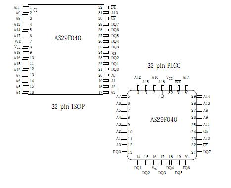
The AS29F040 is a 4-megabit, 5-volt-only Flash memory device organized as 512K bytes of 8 bits each. For flexible erase an program capability, the 4 megabits of data is divided into eight 64K-byte sectors. The *8 data appears on DQ0DQ7. The AS29F040 is offered in JEDEC standard 32-pin TSOP and 32-pin PLCC packages. This device is designed to be programmed an erased in-system with a single 5.0V VCC supply. The device can also be reprogrammed in standard EPROM programmers.
The AS29F040 offers access times of 55/70/90/120/150 ns, allowing 0-wait state operation of high-speed microprocessors. To eliminate bus contention the device has separate chip enable (CE), write enable (WE), and output enable (OE) controls
The AS29F040 is fully compatible with the JEDEC single power supply Flash standard. Write commands to the command register use standard microprocessor write timings. An internal state machine uses register contents to control the erase and programming circuitry. Write cycles also internally latch addresses and data needed for the programming and erase operations. Read data operates from the device in the same manner as other Flash or EPROM devices. The program command sequence is used to invoke the automated on-chip programming algorithm that automatically times the program pulse widths and verifies proper cell margin. The erase command sequence is used to invoke the automated on-chip erase algorithm that preprograms the sector if it is not already programmed before executing the erase operation, times the erase pulse widths, and verifies proper cell margin.
Sector erase architecture allows specified sectors of memory to be erased and reprogrammed without altering data in other sectors . A sector typically erases and verifies within 1.0 seconds. Hardware sector protection disables both program and erase operations i n any or all combinations of the eight sectors. The device provides true background erase with Erase Suspend, which puts erase operations on hold to either read data from or program data to a sector that is not being erased. The chip erase command will automatically erase all unprotected sectors.
A factory shipped AS29F040 is fully erased (all bits = 1). The programming operation sets bits to 0. Data is programmed into the array one byte at a time in any sequence and across sector boundaries. A sector must be erased to change bits from 0 to 1. Erase returns all bytes in a sector to the erased state (all bits = 1). Each sector is erased individually with no effect on other sectors.
The device features single 5.0V power supply operation for read, write, and erase functions. Internally generated and regulate voltages are provided for the program and erase operations. A low VCC detector automatically inhibits write operations during power transtitions. DATA polling of DQ7 or toggle bit (DQ6) may be used to detect end-of-program or erase operations. The device automatically resets to read mode after program and/or erase operations are completed.
The AS29F040 resists accidental erasure or spurious programming signals resulting from power transitions. Control register architecture permits the alteration of memory contents only after successful completion of specific command sequences. During power up, the device is set to read mode with all program and/or erase commands disabled when VCC is less than VLKO (lockout voltage). The command registers are not affected by noise pulses of less than 5 ns on OE, CE, or WE. CE and WEmust be logical zero and OE a logical one to initiate write commands.
The AS29F040 uses Fowler-Nordheim tunnelling to electrically erase all bits within a sector simultaneously. Bytes are programme one at a time using the EPROM programming mechanism of hot electron injection.
AS29F040 Maximum Ratings
Parameter
Min
Symbol
Max
Unit
Input voltage (Input or DQ pin)
VIN
2.0
+7.0
V
Input voltage (A9 pin, OE)
VIN
2.0
+13.0
V
Power supply voltage
VCC
-0.5
+5.5
V
Operating temperature
TOPR
55
+125
°C
Storage temperature (plastic)
TSTG
65
+125
°C
Short circuit output current
IOUT
-
-200
mA
NOTE: Stresses greater than those listed under Absolute Maximum Ratings may cause permanent damage to the device. This is a stress rating only and functional operation of the device at these or any other conditions outside those indicated in the operational sections of this specification is not implied. Exposure to absolute maximum rating conditions for extended periods may affect reliability. Includes all pins except VCC. Test conditions: VCC = 5.0V, one pin at a time.
AS29F040 Features
• Organization:512K words × 8 bits • Industrial and commercial temperature • Sector architecture - Eight 64K byte sectors - Erase any combination of sectors or full chip • Single 5.0±0.5V power supply for read/write operations • Sector protection • High speed 55/70/90/120/150 ns address access time • Automated on-chip programming algorithm - Automatically programs/verifies data at specified address • Automated on-chip erase algorithm - Automatically preprograms/erases chip or specified sectors • 10,000 write/erase cycle endurance • Low power consumption - 30 mA maximum read current - 60 mA maximum program current - 400 µA typical standby current • JEDEC standard software, packages and pinouts - 32-pin TSOP - 32-pin PLCC • Detection of program/erase cycle completion -DQ7 DATA polling - DQ6 toggle bit • Erase suspend/resume - Supports reading data from or programming data to a sector not being erased • Low VCC write lock-out below 2.8V