Want to post a buying lead? If you are not a member yet, please select the specific/related part number first and then fill the quantity and your contact details in the "Request for Quotation Form" on the left, and then click "Send RFQ".Your buying lead can then be posted, and the reliable suppliers will quote via our online message system or other channels soon.
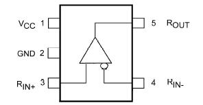
This single receiver is designed for high speed interconnects utilizing Low Voltage Differential Signaling (LVDS) technology. The receiver translates LVDS levels, with a typical differential input threshold of 100 mV, to LVTTL signal levels. LVDS provides low EMI at ultra low power dissipation even at high frequencies. This device is ideal for high speed transfer of clock or data.
The FIN1002 can be paired with its companion driver, the FIN1001, or with any other LVDS driver.
FIN1002 Maximum Ratings
Supply Voltage (VCC)......................................... −0.5V to +4.6V DC Input Voltage (RIN+, RIN−) ..........................−0.5V to +4.6V DC Output Voltage (DOUT) ...................................−0.5V to +6V DC Output Current (IO) ...................................................16 mA Storage Temperature Range (TSTG) ...........−65°C to +150°C Max Junction Temperature (TJ) ......................................150°C Lead Temperature (TL) (Soldering, 10 seconds) .................................................260°C
FIN1002 Features
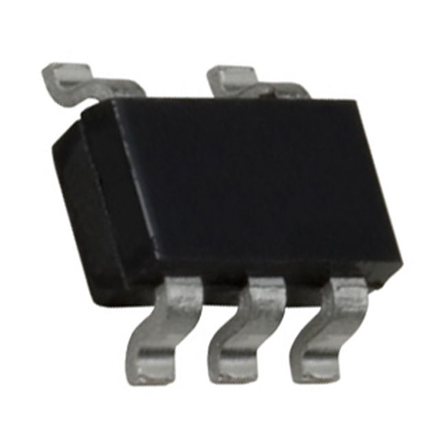
• Greater than 400Mbs data rate • 3.3V power supply operation • 0.4ns maximum pulse skew • 2.5ns maximum propagation delay • Bus pin ESD (HBM) protection exceeds 10kV • Power-Off over voltage tolerant input and output • Fail safe protection for open-circuit and non-driven,shorted or terminated conditions • High impedance output at VCC < 1.5V • Meets or exceeds the TIA/EIA-644 LVDS standard • 5-Lead SOT23 package saves space