

Appliance
RC Buffer Circuit Design in Switching Power Supply
Published:2011/6/22 4:32:00 Author:Amy From:SeekIC
In structure of switching power supply topology with a transformer, when switch turns off, the loss caused by voltage and current overlap is the major part of switching power loss, while in the circuit, stray inductance and stray capacitance, as power switch off, will cause over-voltage and oscillation in the circuit. If the peak voltage is too high, it will damage the switch. Meanwhile, the existence of the oscillation will make the output ripple increase. To reduce the turn-off losses and peak voltage, you need to add buffer circuit in parallel at both ends of switch to improve the circuit performance.
The main functions of the buffer circuit are: first, to reduce turn-on or turn-off losses; secondly, to reduce the voltage or current peak value; thirdly, to reduce dV / dt or dI / dt. Since the MOSFET current falls quickly, it’s turn-off losses quite little. Although MOSFET adopts turn-off snubber circuit, its role is not to reduce the turn-off losses, but to reduce the transformer leakage inductance peak voltage. In this paper, we are mainly discussing MOSFET turn-off snubber circuit.
When developers design RC buffer circuit, they must be familiar with the main circuit topology used in the case. Figure l shows the snubber circuit with forward converter with composition of RC. As shown in the Figure, when Q turns off, the collector voltage starts to rise to 2Vdc, and the rising speed of collector voltage is limited by the capacitor C, and meantime, the rising voltage and falling current overlap is reduced, thus to reduce the Q-switch loss. And before the next switch turns off, C must fully discharges the fully charged voltage 2Vdc, and the discharge path is C, Q, and R. 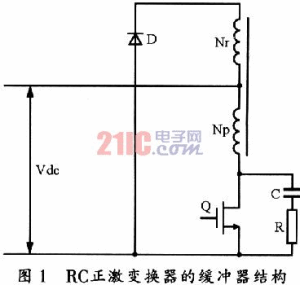
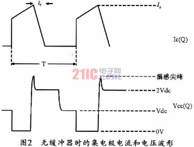
Assuming the switch does not have the buffer circuit, shown in Figure 1, the reset winding of forward converter is the same as primary winding turns. Thus, when Q turns off instantly, the energy stored in the magnetizing inductance and leakage inductance is released. Meantime, the voltage at the primary winding reverses polarity and forward converter switch collector voltage quickly rises to 2Vdc. Meanwhile, the excitation current flows through the diode D reset winding, and finally reduce to zero. The voltage at both ends of Q drop to 0Vdc. Figure 2 shows the switch collector current and voltage waveforms. As we can see, when Q is off, the switch without snubber circuit’s leakage inductance voltage peak is very great, and so does the resulting turn-off losses. Even the switch tube will be burned under severe situation. Therefore, the buffer circuit must be added in switch tube. The related integrated circuit is 2101_IMC.
Reprinted Url Of This Article: http://www.seekic.com/blog/Appliance/2011/06/22/RC_Buffer_Circuit_Design_in_Switching_Power_Supply.html
Print this Page | Comments | Reading(1201)
Article Categories
New published articles
· Imagination works with TSMC to develop FinFET process
Author:Ecco Reading(48994)
· XMOS pushes event-driven MCUs with lower price
Author:Ecco Reading(4235)
· Intel brings upgraded 32-nm SoC for smartphones
Author:Ecco Reading(3956)
· Micron pushes TLC 128-Gbit NAND flash
Author:Ecco Reading(4697)
· Intel will stop supplying desktop motherboards
Author:Ecco Reading(6034)
· Processor market was expected to regain strength in 2013
Author:Ecco Reading(4031)
· It was reported that TSMC sales fall steeply
Author:Ecco Reading(3701)
· Cisco, NXP work with auto wireless startup
Author:Ecco Reading(4368)
· Micron was impacted by manufacturing glitch
Author:Ecco Reading(4720)
· China can make 22-nm transistor by themselves
Author:Ecco Reading(4586)
· Chip market rebound is coming, according to survey
Author:Ecco Reading(4460)
· Sony, Toshiba will spend more on chips, iSuppli reports
Author:Ecco Reading(4019)
· Qualcomm becomes the 13th company to join NFC Forum board
Author:Ecco Reading(6879)
· TSMC increases building work for FinFET fab
Author:Ecco Reading(4546)
· TI plans to cut 1,700 jobs in OMAP shift
Author:Ecco Reading(5425)