

Industry News
Sony plans to spend $1-billion on stacked CMOS sensor
Published:2012/6/25 2:06:00 Author:Ecco From:SeekIC
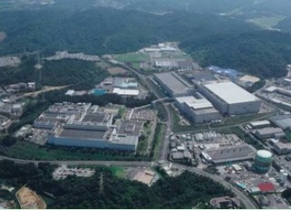
According to Sony Corp., it has planed to spend about 80 billion yen (about $1 billion) by September 2013 in expanding its manufacturing capacity for stacked CMOS image sensors.
Sony Semiconductor has already assigned 45 billion yen investment on Nagasaki wafer fab, and the investment will be finished on March 31, 2013. The company will increase Sony’s production capacity for image sensors to 60,000 wafers per month.
Sony announced that, stacked CMOS image sensors attach the back-illuminated sensors on to ICs that perform signal processing, rather than using substrates to support both the back-illuminated CMOS image sensors and processing IC. The sensors have smaller size which allows more compact size for digital cameras and mobile devices.
However, Sony wishes that the billion-dollar cost can solidify Sony’s position as the largest maker of CMOS image sensors and address the rapidly increasing demand for image sensors for use in smartphones and tablet computers.
Reprinted Url Of This Article: http://www.seekic.com/blog/IndustryNews/2012/06/25/Sony_plans_to_spend_1_billion_on_stacked_CMOS_sensor.html
Print this Page | Comments | Reading(506)
Article Categories
New published articles
· Imagination works with TSMC to develop FinFET process
Author:Ecco Reading(30015)
· XMOS pushes event-driven MCUs with lower price
Author:Ecco Reading(3456)
· Intel brings upgraded 32-nm SoC for smartphones
Author:Ecco Reading(3178)
· Micron pushes TLC 128-Gbit NAND flash
Author:Ecco Reading(3649)
· Intel will stop supplying desktop motherboards
Author:Ecco Reading(5225)
· Processor market was expected to regain strength in 2013
Author:Ecco Reading(3242)
· It was reported that TSMC sales fall steeply
Author:Ecco Reading(3385)
· Cisco, NXP work with auto wireless startup
Author:Ecco Reading(3525)
· Micron was impacted by manufacturing glitch
Author:Ecco Reading(3932)
· China can make 22-nm transistor by themselves
Author:Ecco Reading(3701)
· Chip market rebound is coming, according to survey
Author:Ecco Reading(3673)
· Sony, Toshiba will spend more on chips, iSuppli reports
Author:Ecco Reading(3708)
· Qualcomm becomes the 13th company to join NFC Forum board
Author:Ecco Reading(6023)
· TSMC increases building work for FinFET fab
Author:Ecco Reading(3686)
· TI plans to cut 1,700 jobs in OMAP shift
Author:Ecco Reading(4473)