

Project Solutions
ATX Power Supply Tester: check all voltages (2)
Published:2011/8/14 22:34:00 Author:Li xiao na From:SeekIC
By Ton Giesberts
A look at the circuit
An ATX power supply has a total of 6 output voltages, which all have to be tested: +3.3 V, +5 V, +5 V for standby. +12 V. +5 V and +12 V. The standby voltage (-5VSB) is always present as long as the mains is connected. This voltage is therefore used as the supply for the tester (Figure 1). LED Dl is driven directly from the - 5VSB supply and hence indicates that the mains is turned on and that the power supply has at least a working standby voltage. 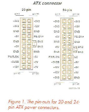
The power supply is turned on by closing switch S2. This pulls pin PS_ON sufficiently low via R56. According to the specification this pin should be <0.8 V at 1.6 mA. A value of 470Ω for R56 achieves this. The PWR_ON output, also called PWRGOOD or PWR_OK. is used by the power supply to show that the most important outputs { +12 V, +5 V and +3.3 V) are within their limits and can supply a nominal current. When this signal is active, D2 lights up. Since this output can only source 200 μA at a minimum voltage of 2.4 V, a buffer stage consisting of R11. R12 and Ti has been added. Once the mains is turned on (and Dl and D2 are lit). SI is used to select the voltage that is connected to the input of amplifier IC1b.
S1 is a 2-pole 8-way rotary switch (it has to be a break-before-make type. otherwise you’ll introduce shorts in the outputs). The first switch selects the supply voltage to be tested. The common output of this switch is also connected to a PCB pin (via a 100 Q resistor for protection). It is possible to connect a small voltmeter module to this pin. so that the absolute value of the selected voltage can be seen. Next to the connection for the meter (Ml) is an extra PCB pin with +5 V for the voltmeter module.
The selected voltage makes its way via the common of Sib to one of the potential dividers connected to the inputs of IC1b.
Each resistor combination gives the right amount of attenuation to the chosen voltage such that the output of IC1b will be a nominal 2.5 V at every position of S1. There is no need for a symmetrical power supply to measure negative voltages because IC1b is a rail-to-rail type opamp. With positive voltages IC1b functions as a non-inverting buffer. The two negative supply voltages are inverted and attenuated.
We now take a small jump to the tolerance LEDs in the circuit (D3-D8). According to the ATX specification all voltages should be within ±5%, with the exception of -12 V, which may be =10:i. We have therefore chosen four tolerance ranges that are covered by the LEDs: <5% (green LED D3), 5-107: (yellow LED D4). 10-20%; (red LED D5) and >20% (second red LED D6). The range division at 10:: was used to give you the choice whether to accept that deviation or not. A difference of more than 20% is not acceptable in any case.
These LEDs are driven by comparators IC3b-d, which have their inverting inputs connected to a potential divider (R45-R48 and PI). This determines the tolerance ranges with respect to the 2.5 V reference voltage. PI is used to set the reference levels as accurately as possible.
This just leaves the section that joins the output signal from IC1b to the LEDs. This output signal is nominally 2.5 V and may be a bit more or less when it deviates. But the comparator circuit built round IC3b-d can only indicate negative differences. To get round this problem IC1a inverts the output signal from IC1b. This is followed by an analogue switch that can be controlled using a digital signal. This switch is part of IC2 (a triple analogue multiplexer). The output signal from IC1b and the inverted one from IC1a are connected to inputs YO and Yl of an analogue switch (pins 2 and 1 on IC2). The output of IC1a is also connected to opamp IC3a, which acts as a comparator and compares the signal with the 2.5 V reference voltage. The output of IC3a acts as the control signal for the analogue switch. When the deviation is negative (<2.5 V), IC3a switches pin 2 of IC2 to the output (pin 15), which is connected to the comparators. When the deviation is positive (>2.5 V), the inverted signal (pin 1) is connected to pin 15. In this way LEDs D3-D6 always show the deviation com-pared to the nominal value. The output of comparator IC3a is also connected to two LEDs. which indicate if the measured voltage is greater or smaller than the nominal value. The yellow LED (D7) is lit when the voltage is lower and the red LED (D8) indicates that the voltage is higher than the reference voltage.
The 2.5 V reference voltage mentioned a few times previously is supplied by an LM4041DIZ-ADJ (IC4) made by National Semiconductor. This voltage can be adjusted to exactly 2.5 V with preset P2.
All outputs from the ATX power supply are provided with a resistive load, where some outputs are loaded more than others. The +3.3 V and +5 V outputs often require a minimum load for the power supply to operate correctly, and are therefore loaded more heavily. To avoid excessive heat generation we haven’t taken the maximum power from the supply, but have limited it to some 45 W (R1 to R9).
Reprinted Url Of This Article: http://www.seekic.com/blog/project_solutions/2011/08/14/ATX_Power_Supply_Tester__check_all_voltages_(2).html
Print this Page | Comments | Reading(1459)
Article Categories
New published articles
· Imagination works with TSMC to develop FinFET process
Author:Ecco Reading(30170)
· XMOS pushes event-driven MCUs with lower price
Author:Ecco Reading(3461)
· Intel brings upgraded 32-nm SoC for smartphones
Author:Ecco Reading(3181)
· Micron pushes TLC 128-Gbit NAND flash
Author:Ecco Reading(3661)
· Intel will stop supplying desktop motherboards
Author:Ecco Reading(5231)
· Processor market was expected to regain strength in 2013
Author:Ecco Reading(3248)
· It was reported that TSMC sales fall steeply
Author:Ecco Reading(3390)
· Cisco, NXP work with auto wireless startup
Author:Ecco Reading(3530)
· Micron was impacted by manufacturing glitch
Author:Ecco Reading(3935)
· China can make 22-nm transistor by themselves
Author:Ecco Reading(3707)
· Chip market rebound is coming, according to survey
Author:Ecco Reading(3677)
· Sony, Toshiba will spend more on chips, iSuppli reports
Author:Ecco Reading(3714)
· Qualcomm becomes the 13th company to join NFC Forum board
Author:Ecco Reading(6028)
· TSMC increases building work for FinFET fab
Author:Ecco Reading(3692)
· TI plans to cut 1,700 jobs in OMAP shift
Author:Ecco Reading(4478)