

Project Solutions
LPC210x 'ARMEE' DEVELOPMENT BOARD Part 1: an ARM processor survey (3)
Published:2011/8/16 21:40:00 Author:Phyllis From:SeekIC
By Tony Dixon
Overview of the ARM7TDMI core 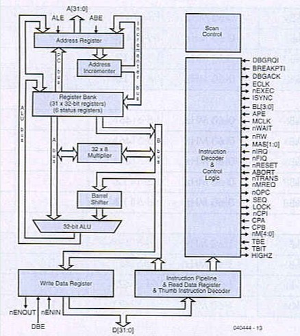
The ARM7 core is a 32-bit Reduced Instruction Set Computer (RISC). It uses a single 32-bit bus for instruction and data. The length of the data can be 8, 16 or 32 bits and the length of the instruction word is 32 bits.
What Does TDMI™ mean?
The ARM7TDMI is an ARM7 core with 4 additional features identified with letter codes, as follows
T: support for the Thumb (16 bit) instruction set.
D: support for debug
M: support for long multiplies
I: include the EmbeddediCE module to support embedded system debugging.
Thumb mode (T)
An ARM instruction is 32-bils long. The ARM7TDMI processor supports a second instruction set that has been compressed into 16-bits, the Thumb instruction set. Faster execution from 16-bit memory and greater code density can usually be achieved by using the Thumb instruction set instead of the ARM instruction set, which makes the ARM7TDMI core particularly suitable for embedded applications. However the Thumb mode has two limitations and these are: Thumb code usually uses more instructions for the same job, so ARM code is usually best for maximising the performance of the time-critical code.
The Thumb instruction set does not include some instructions that are needed for exception handling, so the ARM code needs to be used for exception handling. See ARM7TDMI User Guide for details on the core architecture, the programming model and both the ARM and ARM Thumb instruction sets.
Long multiple (M)
A 32-bit Multiplier function qualifies the core for complex arithmetic tasks usually performed by a DSR The ARM7TDMI instruction set includes four extra instructions that perform 32-bit by 32-bit multiplication with 64-bit result and 32-bit by 32-bit multiplication-accumulation (MAC) with 64-bit result.
Debugging (D)
A special hardware extension allows for Debugging within an application. This is made possible by means of a boundary-scan cell array around the core driven by a JTAG port and a TAP controller.
EmbeddediCE (I)
The EmbeddediCE extends the debugging functions and this module contains the breakpoint and watch point registers that allow the code to be halted for debugging purposes. These registers are controlled through the JTAG test port with the aid of software debugging tools running on a computer. When o breakpoint or watch point is encountered the processor halts and enters debug state. Once in a debug state, the processor registers may be inspected as well as the Flash/EE, SRAM and the Memory Mapped Registers
Reprinted Url Of This Article: http://www.seekic.com/blog/project_solutions/2011/08/16/LPC210x_'ARMEE'_DEVELOPMENT_BOARD__Part_1__an_ARM_processor_survey__(3).html
Print this Page | Comments | Reading(1482)
Article Categories
New published articles
· Imagination works with TSMC to develop FinFET process
Author:Ecco Reading(30178)
· XMOS pushes event-driven MCUs with lower price
Author:Ecco Reading(3461)
· Intel brings upgraded 32-nm SoC for smartphones
Author:Ecco Reading(3181)
· Micron pushes TLC 128-Gbit NAND flash
Author:Ecco Reading(3661)
· Intel will stop supplying desktop motherboards
Author:Ecco Reading(5231)
· Processor market was expected to regain strength in 2013
Author:Ecco Reading(3248)
· It was reported that TSMC sales fall steeply
Author:Ecco Reading(3390)
· Cisco, NXP work with auto wireless startup
Author:Ecco Reading(3530)
· Micron was impacted by manufacturing glitch
Author:Ecco Reading(3935)
· China can make 22-nm transistor by themselves
Author:Ecco Reading(3707)
· Chip market rebound is coming, according to survey
Author:Ecco Reading(3677)
· Sony, Toshiba will spend more on chips, iSuppli reports
Author:Ecco Reading(3714)
· Qualcomm becomes the 13th company to join NFC Forum board
Author:Ecco Reading(6028)
· TSMC increases building work for FinFET fab
Author:Ecco Reading(3692)
· TI plans to cut 1,700 jobs in OMAP shift
Author:Ecco Reading(4478)