

Project Solutions
Part 1: PCB design basics 1
Published:2011/8/24 2:07:00 Author:Amy From:SeekIC
Karol Walraven
What do most electronics engineers enjoy a lot? Designing printed circuit boards, of course! In an irregular series of articles we would like to familiarize you with this subject. We start as simple as possible and it will become more difficult as we progress. Feedback and requests to cover certain topics are encouraged and welcomed!
When you’re just designing a small PCB, it often is not that important where the actual components ore placed. However, there are a few rules of thumb that, when followed, quickly and easily result in a much better PCB. Belter in this context means lower noise in the desired output signal and loss interference with other equipment. The last sentence means, translated into practice: "your amplifier provides a better sound, makes no additional noises when the fridge turns on and does not interfere with your mobile phone".
The following statement is perhaps surprising, but is actually true: "The optimum position of a component on o PCB is for nearly 100% determined by its function in the schematic diagram." That means you cannot avoid thinking about the function of each and every component in the circuit.
Example
We use an amplifier stage as an example. What are the different functionalities that can be distinguished?
In Figure 1, C5 is a decoupling capacitor, which decouples the power supply voltage. The current drawn by ICI will change during operation and C5 ensures that the peak current demand can be delivered. 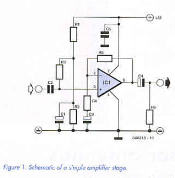
CI is a decoupling capacitor as well, but in this case it serves the purpose of preventing any hum and interference from the power supply from reaching the signal.
C3 is a decoupling capacitor too, but this lime not for the power supply voltage, but for the signal instead. Its function is lo ensure that the inverting input of ICI is connected lo ground, via R4, for AC voltages.
Rule 1: Decoupling components must be placed as dose as is practicable to the nodes that need to be decoupled.
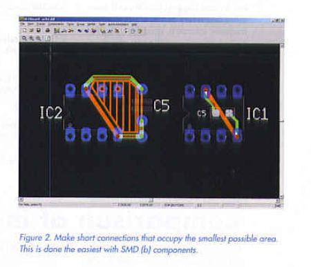
Long traces hove a higher impedance (= resistance for high frequencies) and as a consequence the decoupling will not work as well. The higher the frequency, the more important it becomes to keep the traces shod. Pay close attention! To clarify this a little more, lake a look al Figure 2a .The traces towards and away a/ways form a loop (also when one side of the component is connected lo ground). In the figure we have shaded the area between the traces for clarity. We cannot overemphasize that it is very important lo place the traces in such a way that the shaded area is us small as is possible. If you have to choose between long tracks with a smaller enclosed area or shorter faces with larger enclosed area, then choose the layout with the smallest area" Why that is so we will explain at a later time. It is a little too advanced for the present discussion.
Reprinted Url Of This Article: http://www.seekic.com/blog/project_solutions/2011/08/24/Part_1__PCB_design_basics_1.html
Print this Page | Comments | Reading(1529)
Article Categories
New published articles
· Imagination works with TSMC to develop FinFET process
Author:Ecco Reading(49201)
· XMOS pushes event-driven MCUs with lower price
Author:Ecco Reading(4245)
· Intel brings upgraded 32-nm SoC for smartphones
Author:Ecco Reading(3966)
· Micron pushes TLC 128-Gbit NAND flash
Author:Ecco Reading(4706)
· Intel will stop supplying desktop motherboards
Author:Ecco Reading(6045)
· Processor market was expected to regain strength in 2013
Author:Ecco Reading(4041)
· It was reported that TSMC sales fall steeply
Author:Ecco Reading(3713)
· Cisco, NXP work with auto wireless startup
Author:Ecco Reading(4377)
· Micron was impacted by manufacturing glitch
Author:Ecco Reading(4728)
· China can make 22-nm transistor by themselves
Author:Ecco Reading(4593)
· Chip market rebound is coming, according to survey
Author:Ecco Reading(4470)
· Sony, Toshiba will spend more on chips, iSuppli reports
Author:Ecco Reading(4030)
· Qualcomm becomes the 13th company to join NFC Forum board
Author:Ecco Reading(6890)
· TSMC increases building work for FinFET fab
Author:Ecco Reading(4555)
· TI plans to cut 1,700 jobs in OMAP shift
Author:Ecco Reading(5432)