

Technical Center
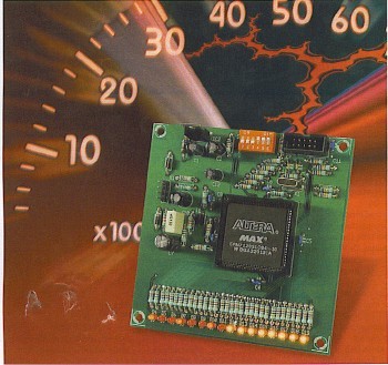
Hands-on CPLDs -Part I: Experimental rev counter (1)
Published:2011/7/20 1:44:00 Author:Li xiao na From:SeekIC
By A. Rosenkranzer
In the past Complex Programmable Logic Devices (CPLDs) have been something of a closed book to most semi-professional electronics enthusiasts but this hands-on series should go some way to help dispel that myth.
Times change. It wasn’t long ago that programmable logic devices (PLDs) were thought to be the preserve of the specialist designer who with the help of expensive development environments and unwieldy software emulators took months to cram large digital designs onto a single PLD. Nowadays the whole process has been simplified to such an extent that the only expensive bit of kit you are likely to need is a PC. An interface adapter is also necessary to connect to the in-circuit programming socket of the CPLD circuit board but its cost is relatively low. When you add to this the fact that the price of the chips themselves have tumbled greatly and the development software is now freely available, these devices start to look attractive even to the hobbyist.
Programmable Logic -An overview
Lift the lid on any piece of modern-day electronic equipment and you will be lucky to find any discrete components from say the 74’ family of logic gates used in the design. Occasionally you may see a clock circuit or bus driver but these are essentially used for driving or buffering and do not have a logic function. High volume consumer products such as computer boards have all the logic functions implemented in ASICs (Application Specific Integrated Circuits). The per-unit cost of an ASIC is quite low but there is also the expensive (one off) mask cost to consider. The equipment manufacturer must be sure of the potential market before a commitment to use ASICs in a design is made.
In the equipment development phase and also for low-volume production ASICs are not cost effective; here the favored technology is the Programmable Logic Device or PLD. These devices started to appear back in the 80’s and since then many more companies have got in on the act to offer bigger and better devices in all sorts of package outline and more recently with lower operating voltages.
The first examples had relatively few registers (flip flops), required a lot of external buffers/drivers and consumed quite a lot of power. On top of this there was also special equipment necessary to program the device. Most of these chips were one-time programmable so that if a mistake was made in programming or some function required modification then the programmed devices could not be reused. On cost alone (development and simulation software together with the programmer device) PLDs were never considered suitable for the hobbyist.
As we said at the beginning times change, PLDs now offer far more gates per package and have become reusable. The real breakthrough came with the ’in system programmable’ devices. As the name suggests these chips are fitted permanently into the finished equipment and can be reprogrammed via a 10-pin JTAG interface connector fitted somewhere on-board. The interface allows several devices to be daisy-chained and programmed from just the one connector. The devices do not require a socket so this has led to an increase in the device pin density right up to the BGA package outline. A few manufacturers still offer devices in the more user-friendly PLCC outline which is more suited to a typical hobbyist project.
The necessary development software from practically every chip manufacturer is now freely available for download from the Internet. A simple piece of hardware like the ByteBlaster from Altera is all that you need to connect a PC to the JTAG connector on the PCB. Regular readers will remember the Byte-Blaster compatible ’Parallel JTAG Interface’ design featured in the September 2002 edition of Elektor Electronics.
CPLDs (Complex PLDs) evolved from PLDs and the next step along the way is FPGAs (Field Program-able Gate Arrays). The main difference besides the increased complexity is that CPLDs (mostly using EEPROM technology) do not lose there programming data when the device is powered down.
In contrast FPGAs must be re-programmed every time they are switched on. Reprogramming is performed automatically from a ’boot device’ (either a serial EEPROM or flash memory) fitted to the PCB. The reason for this is that it is not yet possible to fabricate high-speed EEPROM technology at the necessary cell density required for an FPGA.
The clock speeds of FPGAs can be several hundred megahertz and some manufacturers are offering SERDES technology that pushes the data rate up to 3.7 Gbps (10 Gbps will no doubt be available by the time you read this) these devices include complete processor cores (ARM, NIOS). Dropping the supply voltage down from 5 V to around 1.5 V has also led to reduced power dissipation in the device.
Around 90% of all FPGAs sold are supplied by three manufacturers: Xilinx, Altera and Lattice. FPGAs have an enormous capacity of gates and can be used in thousands of applications. They also do not have the expensive one-off mask costs of an ASIC.
Reprinted Url Of This Article: http://www.seekic.com/blog/technical_center/2011/07/20/Hands_on_CIPtLGJs__Part_I__Experimental_rev_counter.html
Print this Page | Comments | Reading(1073)
Article Categories
New published articles
· Imagination works with TSMC to develop FinFET process
Author:Ecco Reading(48229)
· XMOS pushes event-driven MCUs with lower price
Author:Ecco Reading(4212)
· Intel brings upgraded 32-nm SoC for smartphones
Author:Ecco Reading(3936)
· Micron pushes TLC 128-Gbit NAND flash
Author:Ecco Reading(4676)
· Intel will stop supplying desktop motherboards
Author:Ecco Reading(6019)
· Processor market was expected to regain strength in 2013
Author:Ecco Reading(4013)
· It was reported that TSMC sales fall steeply
Author:Ecco Reading(3682)
· Cisco, NXP work with auto wireless startup
Author:Ecco Reading(4351)
· Micron was impacted by manufacturing glitch
Author:Ecco Reading(4703)
· China can make 22-nm transistor by themselves
Author:Ecco Reading(4567)
· Chip market rebound is coming, according to survey
Author:Ecco Reading(4442)
· Sony, Toshiba will spend more on chips, iSuppli reports
Author:Ecco Reading(4008)
· Qualcomm becomes the 13th company to join NFC Forum board
Author:Ecco Reading(6863)
· TSMC increases building work for FinFET fab
Author:Ecco Reading(4528)
· TI plans to cut 1,700 jobs in OMAP shift
Author:Ecco Reading(5408)